ALLPCB


AllElectroHub Electronics News & Technical Insights
Say Goodbye to Sharp Edges - Inside ALLPCB’s Burr-Free PCB Process
Learn about PCB burrs, their causes, and impacts on electronics. Discover ALLPCB's multi-step process to ensure burr-free circuit boards for reliable performance.
Featured
Latest

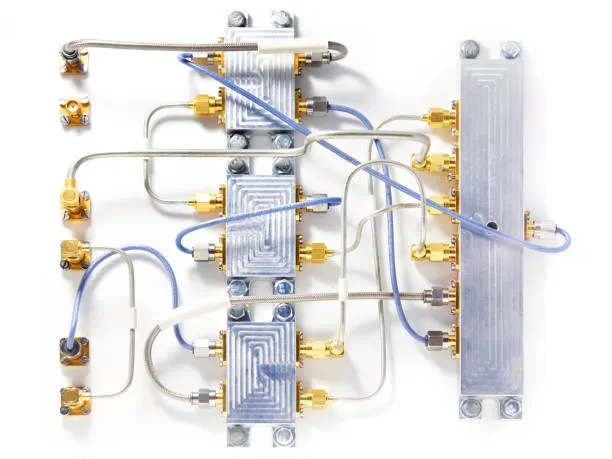
Choosing the Right Connectors for High Frequency 5G PCBs
Learn how to choose 5G PCB connectors for high-frequency mmWave applications. Focus on RF connectors and impedance matching to achieve optimal signal integrity.
PCB Knowledge
Designing for Manufacturability: Black Silkscreen Considerations for PCBs
Master black silkscreen DFM rules to improve PCB visibility and yield. Explore how ink color influences adhesion plus thermal profiles for reliable component placement and inspection.
PCB Knowledge
The Ultimate Guide to Drill Bit Selection for PCB Mechanical Drilling
Select high quality carbide drill bits for PCB mechanical drilling to maintain precision. Learn about bit geometry plus speed and feed parameters for consistent hole quality and board reliability.
PCB Knowledge
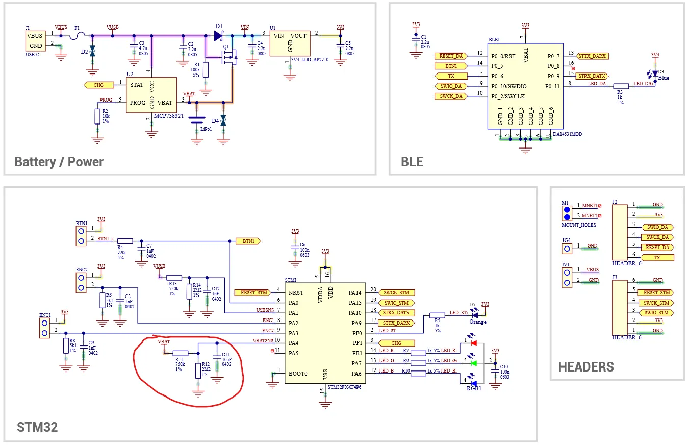
Bluetooth Connectivity for Wearable Health PCBs: Secure and Reliable Data Transmission
Optimize your Bluetooth Low Energy wearable PCB for health monitoring. This expert guide covers RF layout, antenna range, and security to ensure reliable connectivity and extended battery life.
PCB Knowledge
Electric Vehicle PCB Reliability Testing: Ensuring Longevity and Performance
Learn how PCB reliability testing protects electric vehicle systems from vibration and thermal stress. Follow IPC and JEDEC standards to improve board quality and prevent system failures.
PCB Knowledge
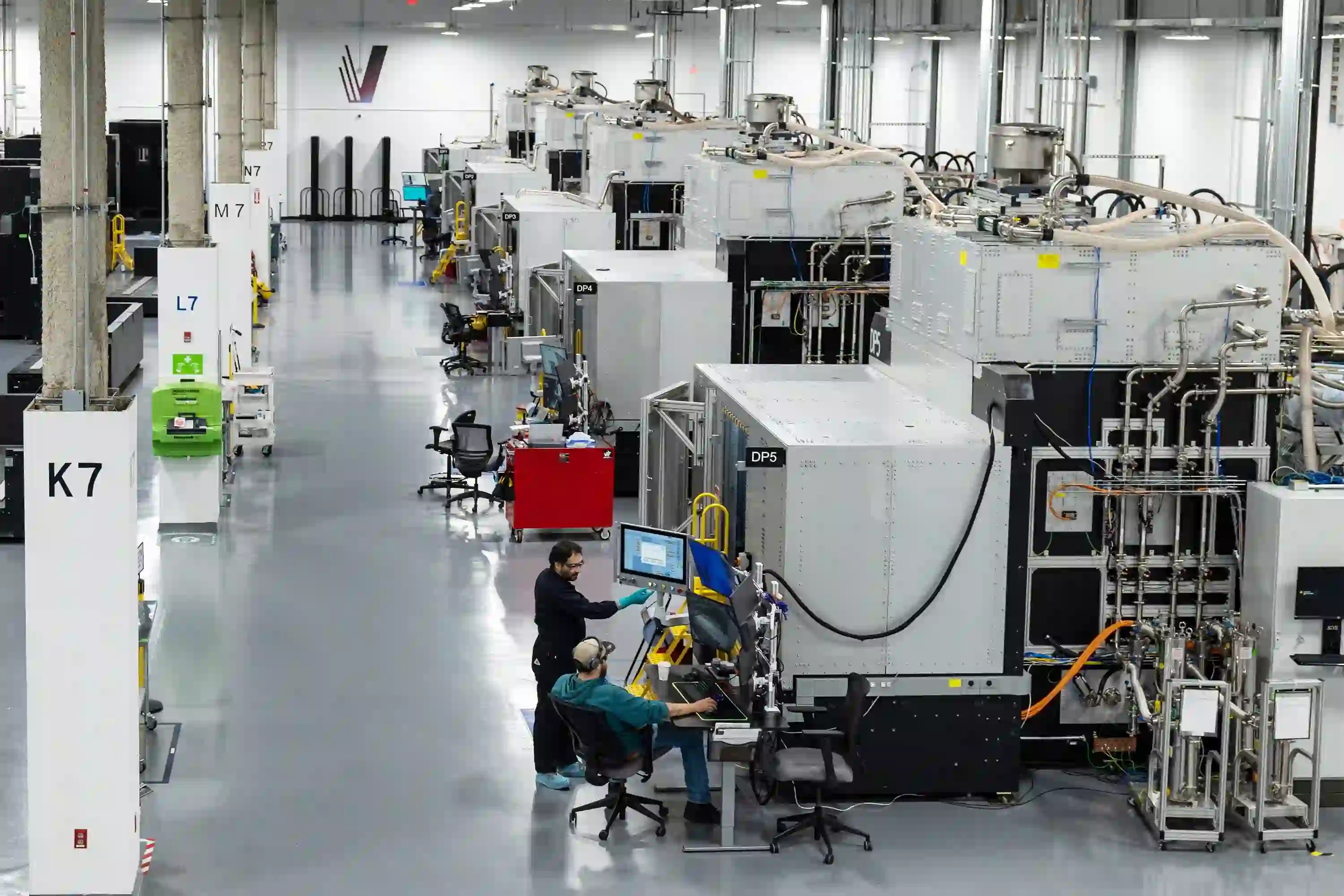
The Future of PCB Technology in Industrial Automation: Trends and Innovations
PCB miniaturization, wireless designs, and advanced materials support progress in industrial automation. Engineers find practical guidance on Industry 4.0 trends along with design and reliability practices for control systems.
PCB Knowledge