ALLPCB


What Is DFM and Why It Matters in PCB Projects
DFM refers to the systematic evaluation of a printed circuit board layout against manufacturing constraints. The DFM process flow begins early in the design cycle and continues through final release. When teams conduct a DFM review, they identify issues such as insufficient spacing, unbalanced copper distribution, or via placement that could cause plating problems. Early attention to these factors lowers scrap rates and shortens time to market. Procurement teams and manufacturing engineers rely on consistent DFM review methodology to maintain predictable production schedules.
Industry standards provide the baseline for these evaluations. Reference documents outline acceptable tolerances for trace width, hole diameter, and board thickness. Following such guidance helps designers avoid features that exceed typical equipment capabilities. The result is a more reliable product that meets both electrical and mechanical requirements without unnecessary complexity.
Technical Principles Behind Effective DFM Review
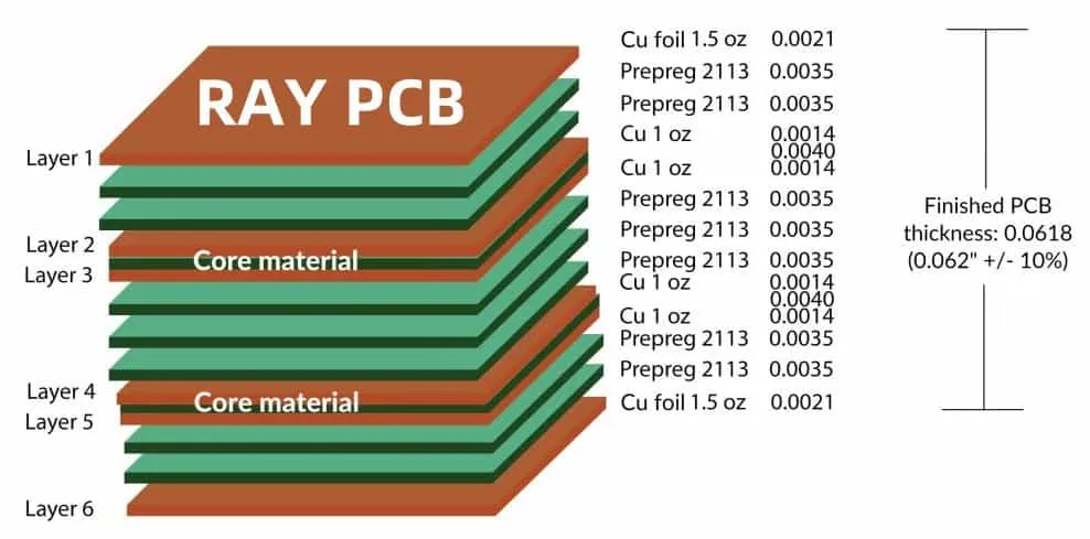
PCB fabrication involves sequential processes that impose specific geometric and material constraints. Trace and space rules derive from etching accuracy and registration tolerances between layers. Via aspect ratios affect plating uniformity inside drilled holes. Copper balance across the board influences thermal expansion during lamination and reflow. Signal integrity considerations intersect with DFM when high-speed traces require controlled impedance that still satisfies minimum feature sizes.
Thermal management introduces additional variables. Large copper pours can create heat sinks that affect soldering profiles on nearby components. Warpage arises when asymmetric stackups or heavy copper areas cause differential expansion during temperature cycling.
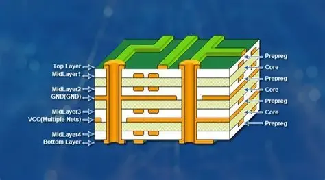
Material selection also shapes DFM outcomes. Laminate choices determine maximum operating temperature and moisture absorption rates. These properties influence both assembly yield and long-term reliability. Designers evaluate these factors alongside electrical performance targets to arrive at a balanced specification.
Step-by-Step PCB Design Review Process
A repeatable DFM review methodology follows a logical sequence of checks. The first step involves importing the design files into a verification tool and running automated rule checks against the fabricator's capability document. Engineers then perform a manual layer-by-layer inspection to catch issues that automated tools may miss, such as overlapping text or silkscreen on pads.
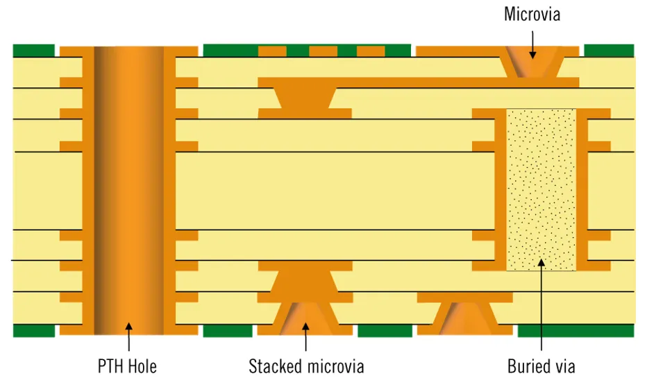
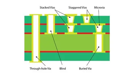
Next comes a review of the drill table and via structures. Minimum hole sizes, annular ring requirements, and via fill decisions receive close attention. Copper distribution analysis follows, with particular focus on large solid areas that may require cross-hatching or thermal reliefs.
Component placement and routing receive scrutiny for assembly compatibility. Clearance around tall parts, orientation consistency for polarized devices, and test point accessibility all factor into the assessment. Thermal profiling considerations ensure that reflow zones will not damage sensitive areas. The final stage compiles findings into a prioritized list for design revision.
Best Practices for Conducting Thorough DFM Reviews
Successful teams maintain a living checklist that evolves with each new board technology. They involve manufacturing engineers early, often during schematic capture, to surface constraints before layout begins. Documentation of every decision, including the rationale for deviating from standard rules, supports traceability and future audits.
Collaboration between design and production groups reduces miscommunication. Regular design review meetings allow real-time feedback on proposed changes. Version control of both layout files and capability documents prevents use of outdated specifications.
When issues surface, engineers evaluate multiple mitigation options rather than accepting the first workaround. For example, adjusting trace routing may resolve a spacing violation while preserving impedance targets. Documentation of accepted deviations helps downstream teams understand intentional compromises.
Common Challenges and Practical Mitigation Approaches
Designers frequently encounter conflicts between electrical performance goals and manufacturing limits. High-density interconnect requirements can push feature sizes below standard capabilities, requiring sequential lamination or alternative via technologies. In such cases, the DFM review methodology guides selection of the least disruptive compromise.
Board warpage during assembly often traces back to asymmetric copper or uneven dielectric distribution. Mitigation includes symmetric stackup planning and strategic use of copper balancing features.
Signal integrity and DFM sometimes compete when differential pairs require tight coupling that conflicts with minimum spacing rules. Careful via placement and reference plane continuity help satisfy both sets of requirements. Consistent application of these practices across multiple projects builds institutional knowledge that accelerates future reviews.
Conclusion
A disciplined approach to PCB design review steps delivers measurable improvements in yield and reliability. Integrating DFM process flow considerations from the earliest layout decisions reduces the frequency of engineering change orders. Teams that apply a consistent DFM review methodology produce designs that transition smoothly from prototype to volume production. Continued attention to evolving standards and process capabilities keeps the methodology current. The cumulative effect supports faster development cycles and more predictable manufacturing outcomes.
FAQs
Q1: What are the essential PCB design review steps within a typical DFM process flow?
A1: The essential steps include automated rule checking against fabricator capabilities, manual layer-by-layer inspection, drill and via analysis, copper distribution review, component placement verification, and compilation of a prioritized revision list. Each step builds on the previous one to create a comprehensive assessment. Following this sequence ensures that both fabrication and assembly constraints receive attention before files are released.
Q2: How does effective PCB design review improve manufacturing outcomes?
A2: Effective PCB design review identifies geometric and material issues early, allowing corrections before tooling and production begin. This reduces scrap, shortens prototype iterations, and improves first-pass yield. The process also documents decisions that support traceability and future design reuse.
Q3: What role does DFM review methodology play when high-speed signals are present?
A3: DFM review methodology evaluates trace geometry, via placement, and reference plane integrity alongside electrical requirements such as controlled impedance. Engineers balance minimum feature sizes with coupling needs and thermal relief strategies. The result maintains signal integrity while remaining within standard manufacturing tolerances.
Q4: Why should teams involve manufacturing engineers during early PCB design review steps?
A4: Early involvement surfaces process-specific constraints before significant layout effort occurs. Manufacturing input helps avoid features that exceed equipment capabilities or require expensive special processes. This collaboration produces designs that align with actual production realities from the outset.
References
IPC-2221B — Generic Standard on Printed Board Design. IPC, 2012
IPC-6012E — Qualification and Performance Specification for Rigid Printed Boards. IPC, 2017
J-STD-001G — Requirements for Soldered Electrical and Electronic Assemblies. IPC, 2017