ALLPCB


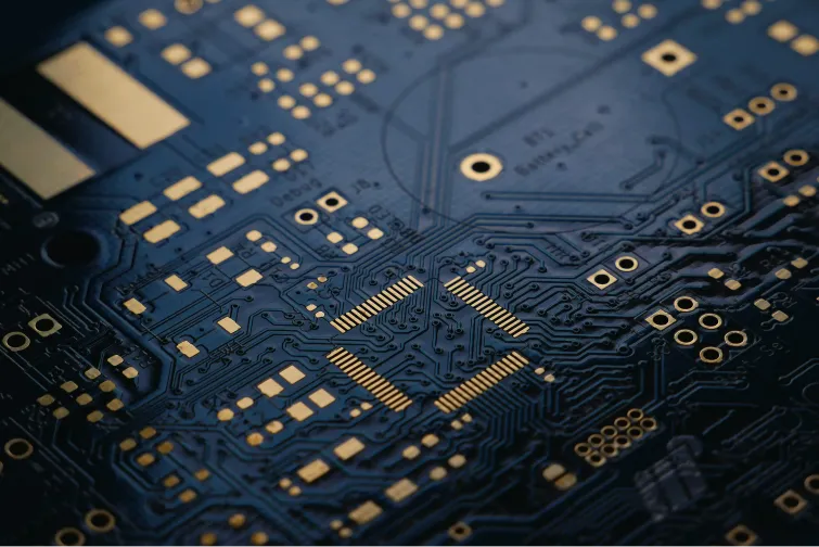
Printed Circuit Boards (PCBs) are the lifeblood of modern electronics, enabling everything from wearable devices to aerospace systems. However, creating a PCB that performs as intended is only part of the equation—ensuring it can be manufactured efficiently, reliably, and cost-effectively is just as vital. This is where PCB design for manufacturing (DFM) steps in. By aligning your design with production realities, PCB DFM minimizes errors, reduces costs, and accelerates time-to-market. In this comprehensive guide, we'll explore the intricacies of PCB design for manufacturing, equipping engineers with the knowledge and tools to optimize their designs for success.
For engineers, the challenge is clear: a design flaw caught late can spiral into delays, rework, or product failures. Whether you're tackling a high-speed RF board or a compact medical device, mastering PCB DFM principles can transform a promising schematic into a production-ready masterpiece. Let's dive into the details and uncover how to make your next PCB design both brilliant and buildable.
What Is PCB Design for Manufacturing (DFM)?
PCB DFM, or Design for Manufacturability, is the practice of tailoring your PCB layout to suit the capabilities and constraints of fabrication and assembly processes. It's about foresight—anticipating manufacturing challenges like etching tolerances or soldering limitations and addressing them during the design phase. Rather than handing off a design and hoping for the best, PCB design for manufacturing ensures your board transitions seamlessly from CAD software to the factory floor.
Why is this critical? A design that overlooks DFM might include vias too small to drill accurately or solder pads too close for reliable assembly. Such issues can lead to a 20-30% increase in scrap rates, push production costs up by 15%, or delay schedules by weeks. By embedding PCB DFM principles early, you create a design that's not only functional but also practical to produce at scale—whether you're building ten units or ten thousand.
Key Principles of PCB DFM
To excel in PCB design for manufacturing, engineers must focus on a handful of foundational principles. Below, we break these down with technical specifics and real-world implications.
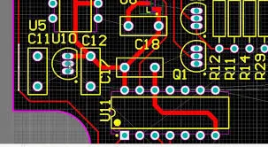
1. Component Placement and Orientation
Effective component placement sets the stage for manufacturability. Crowding components—like placing 0603 capacitors within 0.1 mm of each other—can confuse pick-and-place machines, increasing the risk of misalignment or defects like tombstoning (where one end lifts during soldering). A safe rule of thumb? Maintain at least 0.2 mm clearance for small SMDs and 0.5 mm for larger ICs like QFPs.
Orientation streamlines PCB assembly. Aligning all polarized components (e.g., diodes or electrolytic capacitors) in the same direction—say, positive terminals facing east—cuts programming time for automated equipment by up to 10%. Grouping similar components also helps: clustering resistors or decoupling capacitors can reduce pick-and-place cycles, shaving 15-20% off assembly time for complex boards.
2. Trace Width and Spacing
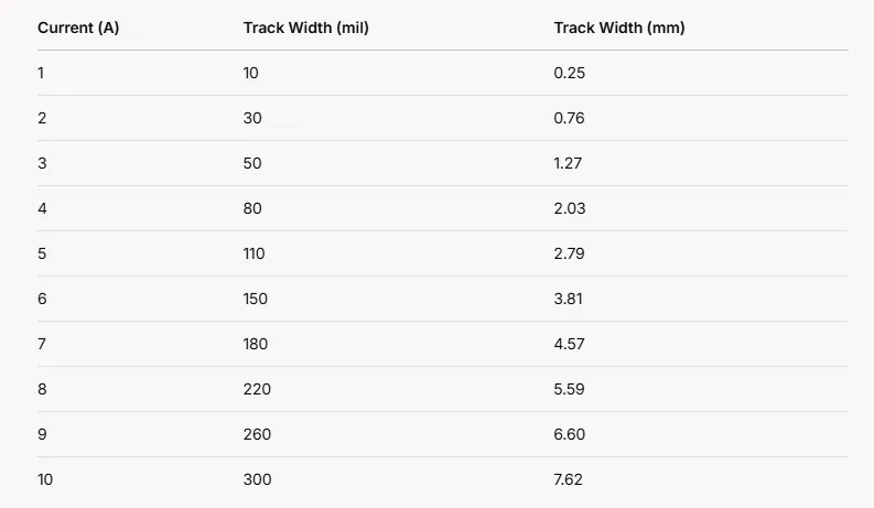
Trace design balances electrical performance with fabrication feasibility. For a 1 oz copper layer carrying 5 amps, the IPC-2152 standard suggests a trace width of 0.125 inches to keep temperature rise below 10°C. Narrower traces—say, 3 mils—push the limits of standard etching processes, risking under-etching or opens. Most fabricators recommend a minimum of 6 mils for outer layers to ensure reliability.
Spacing is just as crucial. A 4-mil gap between traces might work in theory, but etching tolerances (±1 mil) could lead to shorts. For high-voltage designs (e.g., 300V), spacing should jump to 0.06 inches to prevent dielectric breakdown. Controlled impedance traces—like 50-ohm lines for RF signals—demand even tighter control, often requiring a dielectric thickness of 0.008 inches and a tolerance of ±10%.
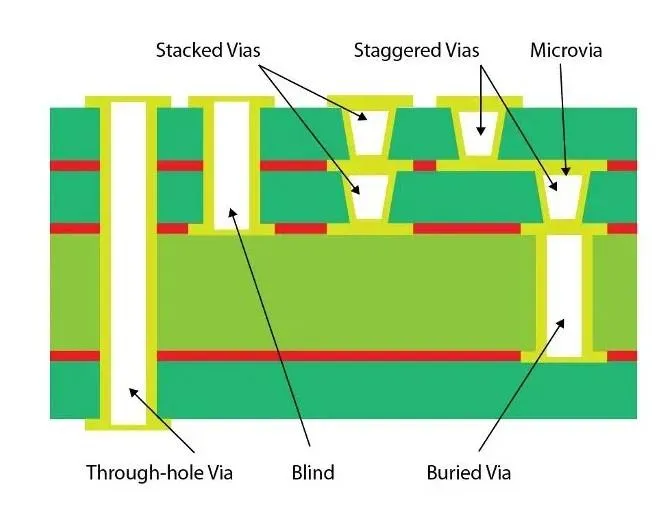
3. Via Design and Placement
Vias are the highways between PCB layers, but their design impacts cost and manufacturability. Standard through-hole vias (0.3 mm diameter) are cost-effective but consume space. Microvias (<0.15 mm) shine in HDI designs, supporting densities up to 20% higher, though they require laser drilling—adding 15-25% to fabrication costs. Blind or buried vias save real estate but complicate stackups, potentially doubling lamination steps.
Placement matters too. Vias within 8 mils of a pad can cause drill breakout, weakening solder joints. Adding teardrop pads—extending the annular ring by 50%—increases mechanical strength, especially in flex PCBs where bending stress peaks at 0.02 inches of deflection.
4. Thermal Management
Heat is a silent killer of PCB reliability. High-power components like MOSFETs or BGAs need thermal reliefs—typically 0.3 mm wide spokes—around pads to balance heat flow during reflow soldering. Without them, uneven cooling can cause cold joints or reduce solder joint lifespan by 30%. For a 10W component, a copper pour of 2 square inches can drop temperatures from 120°C to 80°C, staying within FR-4's 130°C limit.
In multi-layer boards, a dedicated ground plane can cut thermal resistance by 25-35%, dissipating heat across 4-6 layers. Ignoring this risks warpage—0.01 inches of bowing per inch of board length—or premature component failure.
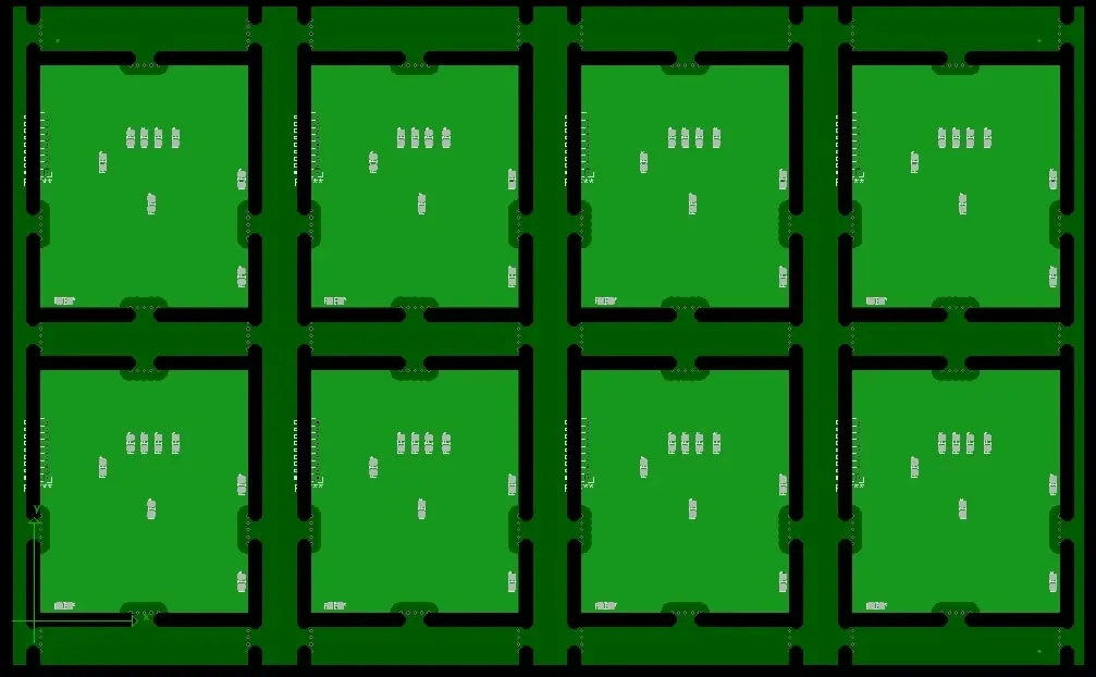
5. Panelization and Edge Clearance
Panelization maximizes material use, but poor planning invites trouble. Copper features within 0.015 inches of the board edge risk damage during PCB depanelization (e.g., V-scoring or routing). A 0.1-inch rail with mouse bites or tabs ensures structural integrity, while a 2x4 array can boost material efficiency by 12% for 2-inch square boards.
Complex arrays with mixed board sizes might save space but increase setup time by 20%. Stick to uniform grids unless volume justifies the complexity.
Advanced PCB DFM Techniques
For cutting-edge designs—like HDI or flex PCBs—standard DFM isn't enough. Here's how to push PCB design for manufacturing further.
1. High-Density Interconnect (HDI) Design
HDI boards pack more functionality into smaller footprints, using microvias and fine-pitch components (e.g., 0.4 mm BGA spacing). DFM requires tighter tolerances: 3-mil traces and 4-mil spaces are common, demanding advanced photolithography. Staggered microvias—offset by 0.1 mm—reduce stress versus stacked vias, improving yield by 10%.
2. Flexible and Rigid-Flex PCBs
Flex PCBs need wider bend radii (e.g., 10x the board thickness) to avoid copper cracking. For a 0.01-inch thick flex layer, that's a 0.1-inch radius. DFM tip: use hatched copper fills instead of solid planes to cut stiffness by 20%, easing assembly into tight enclosures.
3. Signal Integrity Optimization
High-speed designs (e.g., 5 Gbps signals) demand controlled impedance and minimal crosstalk. A 50-ohm trace might need a 0.005-inch width on a 0.008-inch dielectric, with 0.01-inch spacing to adjacent traces. Differential pairs should match lengths within 5 mils to avoid skew, critical for USB 3.0 or PCIe.
Common PCB DFM Mistakes and How to Avoid Them
Even experienced engineers can trip over PCB DFM hurdles. Here are the top mistakes and how to sidestep them.
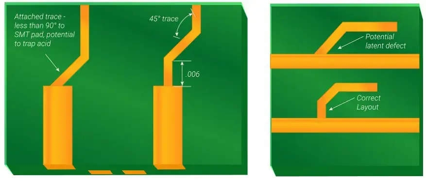
1. Acid Traps
Sharp trace angles (<90°) trap etchant, over-etching copper and raising defect rates by 5-10%. Route at 45° or use curved transitions. Modern etchants mitigate this, but old habits die hard—stick to smooth paths.
2. Insufficient Annular Rings
A 0.3 mm drill with a 0.4 mm pad leaves a 0.05 mm ring—too thin for reliable plating. Aim for 0.1 mm minimum (e.g., 0.5 mm pad) to survive thermal cycling (300 cycles at -40°C to 85°C).
3. Overly Complex Stackups
A 16-layer board might impress, but if 10 layers suffice, you're inflating costs by 50%. Simulate signal integrity first—4 layers often handle 1 GHz signals with proper grounding.
4. Ignoring Manufacturer Specs
Designing 3-mil traces for a shop with a 6-mil minimum is a recipe for rejection. Request their capability sheet—most offer 0.1 mm vias and 6/6 mil trace/space as standard.
Case Study: Optimizing a High-Speed PCB with DFM
Consider a real-world example: a 6-layer PCB for a 2.5 Gbps networking device. The initial design had 4-mil traces, 0.2 mm vias, and a cramped BGA footprint. Fabrication flagged issues: the traces risked under-etching, and the vias were too close to pads (6 mils), threatening drill breakout.
After applying PCB DFM:
- Traces widened to 6 mils, maintaining 50-ohm impedance with a 0.01-inch dielectric tweak.
- Vias moved to 10 mils from pads, adding teardrops.
- BGA spacing increased to 0.3 mm, easing assembly.
The result? First-pass yield jumped from 85% to 98%, cutting rework costs by 25% and shrinking lead time from 5 weeks to 3.
Tools and Techniques for Effective PCB DFM
Leveraging the right tools and strategies is key to PCB design for manufacturing success.
1. DFM Software
Altium's DRC catches 90% of spacing errors, while KiCad's 3D viewer spots placement clashes. Run DFM checks for trace width, annular rings, and solder mask slivers (minimum 0.003 inches).
2. Manufacturer Collaboration
Share Gerber files early—fabricators might suggest 8-mil vias over 6 mils for their drills, avoiding a redesign. This cuts iterations by 30-40%.
3. Prototyping and Validation
A quick-turn prototype tests thermal models (e.g., 80°C max for a 5W load) and signal integrity (e.g., eye diagram for 1 Gbps signals). Fix issues here, not in production.
Benefits of Prioritizing PCB DFM
The rewards of PCB DFM are tangible:
- Cost Efficiency: Pre-production fixes cost $100 versus $1,000 post-assembly.
- Speed: DFM slashes design cycles, hitting market 2-3 weeks faster.
- Reliability: Optimized boards achieve 95-99% yields, minimizing recalls.
- Scalability: Designs scale from 100 to 10,000 units without hiccups.
How ALLPCB Supports Your PCB DFM Journey
At ALLPCB, we empower engineers to perfect PCB design for manufacturing. Our quick-turn prototyping delivers boards in 24-48 hours, letting you test DFM tweaks fast. Our team offers free DFM reviews, catching issues like insufficient clearances or thermal risks, so your design shines in production.
Conclusion: Elevate Your PCB Design with DFM
PCB design for manufacturing is the bridge between innovation and execution. By mastering component placement, trace design, thermal management, and advanced techniques, you can craft boards that excel in both performance and production. For engineers, PCB DFM isn't optional—it's the path to reliable, cost-effective, and timely products.
Start your next project with these principles in mind. The payoff? A PCB that's not just a design triumph but a manufacturing success.