 ALLPCB


If you're designing a printed circuit board (PCB) with USB interfaces, ensuring signal integrity and performance is critical. A well-thought-out PCB layout for USB can prevent data loss, reduce noise, and guarantee reliable operation. In this comprehensive guide, we'll dive into the essentials of USB PCB layout, USB routing guidelines, USB impedance control, and USB signal integrity to help you achieve optimal results for your designs.
Whether you're working on USB 2.0, USB 3.0, or the latest USB Type-C interfaces, this blog will walk you through practical tips and best practices. From impedance matching to proper trace routing, we’ve got you covered with actionable advice to elevate your PCB designs.
Why USB PCB Layout Matters for Signal Integrity
USB interfaces are widely used in modern electronics for data transfer and power delivery. However, the high-speed signals involved in USB communication—ranging from 480 Mbps for USB 2.0 to 20 Gbps for USB 3.2 Gen 2x2—make them sensitive to noise, crosstalk, and signal degradation. A poorly designed PCB layout can lead to errors in data transmission, reduced performance, or even complete failure of the USB connection.
The key to avoiding these issues lies in optimizing your USB PCB layout. By following specific USB routing guidelines and maintaining USB impedance control, you can ensure that signals travel without distortion or interference. Let’s explore the core principles and techniques to achieve this.
Key Principles of USB PCB Layout Design
Designing a PCB for USB interfaces requires attention to several fundamental aspects. Below, we break down the most important principles to guide your layout process.
1. Understanding USB Signal Types and Speeds
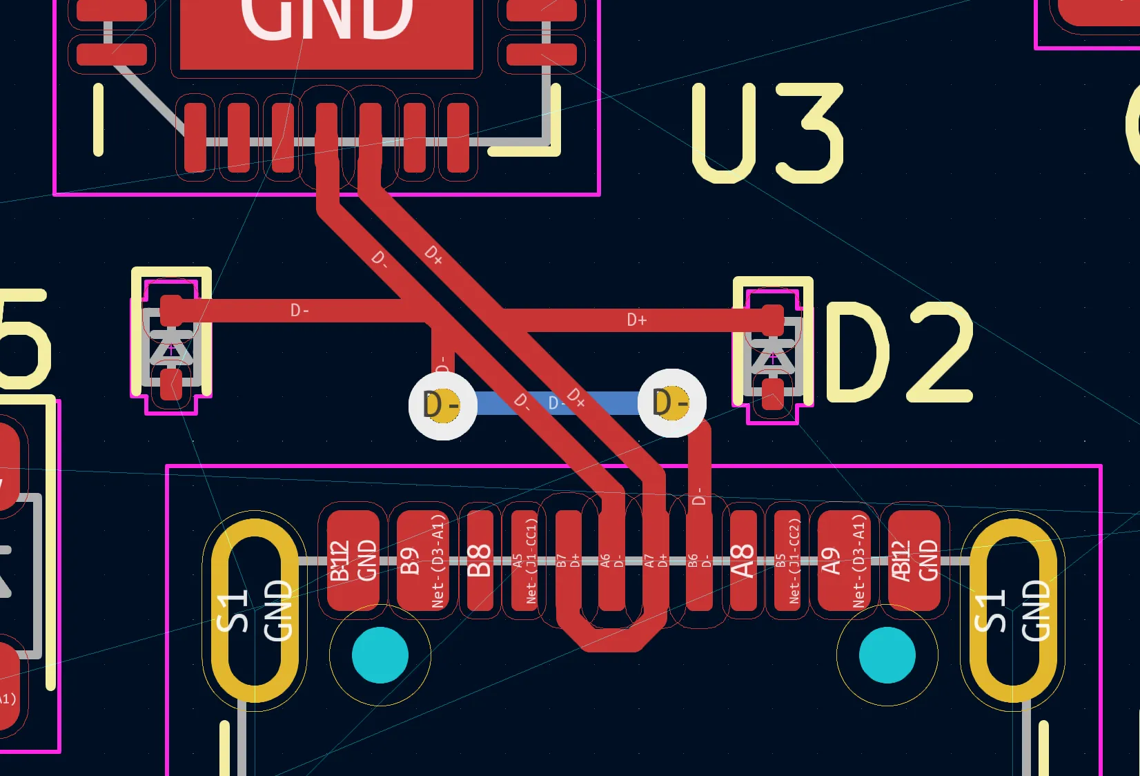
USB interfaces handle differential signals, meaning data is transmitted over two complementary traces (D+ and D- for USB 2.0, or additional pairs for USB 3.0 and beyond). These signals operate at high frequencies, so even small mismatches or interference can cause significant problems.
- USB 2.0: Operates at 480 Mbps with a single differential pair.
- USB 3.0/3.1 Gen 1: Reaches 5 Gbps, adding additional differential pairs for faster data transfer.
- USB 3.2 Gen 2: Supports up to 10 Gbps, requiring even tighter control over signal paths.
- USB Type-C: Combines high-speed data and power delivery, often supporting USB 3.2 or Thunderbolt protocols.
Understanding the speed and signal type of your USB interface helps determine the level of precision needed in your PCB layout. Higher speeds demand stricter USB impedance control and shorter trace lengths to minimize signal loss.
2. USB Impedance Control: Matching for Reliability
Impedance matching is a cornerstone of USB signal integrity. USB differential pairs typically require a characteristic impedance of 90 ohms (±15%) for USB 2.0 and tighter tolerances for USB 3.0 and above. If the impedance is mismatched, reflections can occur, leading to signal distortion and data errors.
To achieve proper USB impedance control:
- Use a PCB stack-up calculator or simulation tool to determine the correct trace width and spacing for your board material and thickness. For example, on a standard FR-4 substrate with a 1.6 mm thickness, a trace width of about 0.2 mm and spacing of 0.2 mm might be needed for a 90-ohm differential pair (values depend on exact stack-up).
- Keep the dielectric constant of your PCB material consistent to avoid impedance variations.
- Route differential pairs over a continuous ground plane to maintain a stable reference and reduce electromagnetic interference (EMI).
3. USB Routing Guidelines: Best Practices for Trace Layout
Routing USB signals on a PCB requires precision to avoid interference and maintain signal integrity. Follow these USB routing guidelines to optimize your layout:
- Keep Traces Short and Direct: Minimize the length of USB signal traces to reduce signal delay and attenuation. For USB 2.0, try to keep traces under 150 mm if possible. For USB 3.0 and above, even shorter lengths (under 100 mm) are ideal.
- Maintain Equal Lengths for Differential Pairs: Ensure that the D+ and D- traces are of equal length to prevent skew, which can cause timing errors. Length mismatches should be less than 0.5 mm for USB 2.0 and even tighter for higher speeds.
- Avoid Sharp Bends: Use 45-degree angles or smooth curves instead of 90-degree bends to prevent signal reflections.
- Isolate USB Traces: Keep USB traces away from high-speed or noisy signals like clocks or power lines to avoid crosstalk. Maintain at least 3x the trace width as separation from other signals.
- Use Ground Planes: Route USB traces over a solid ground plane to provide a low-impedance return path and shield against EMI.
By adhering to these routing guidelines, you can significantly improve the performance of your USB interface and reduce the risk of signal integrity issues.
Advanced Techniques for USB Signal Integrity
Beyond the basics, there are advanced strategies to further enhance USB signal integrity on your PCB. These techniques are especially important for high-speed USB interfaces like USB 3.0 or USB Type-C.
1. Via Placement and Minimization
Vias introduce inductance and capacitance, which can disrupt high-speed USB signals. To minimize their impact:
- Avoid placing vias on USB differential pairs unless absolutely necessary. If unavoidable, use back-drilled or blind vias to reduce stub effects.
- Place vias symmetrically for both traces in a differential pair to maintain balance.
- Keep the number of vias per trace to a minimum—ideally less than two for USB 3.0 signals.
2. Grounding and Decoupling for Noise Reduction
Proper grounding is essential for USB signal integrity. A solid ground plane beneath USB traces helps reduce noise and provides a stable reference for signals. Additionally:
- Place decoupling capacitors (e.g., 0.1 μF and 1 μF) close to USB controller IC pins to filter out power supply noise.
- Use a split ground plane only if absolutely necessary, and ensure proper stitching with vias to connect analog and digital grounds.
3. Shielding for USB Type-C Designs
USB Type-C connectors support high-speed data and power delivery, making them more susceptible to interference. To optimize signal integrity:
- Use shielding layers or enclosures around USB Type-C connectors to block external EMI.
- Route high-speed pairs (like SuperSpeed lines) on inner layers of a multilayer PCB, sandwiched between ground planes for maximum protection.
- Ensure proper termination resistors and capacitors are placed near the connector to manage signal reflections.
Common Mistakes to Avoid in USB PCB Layout
Even with the best intentions, certain mistakes can undermine your USB PCB layout. Here are some pitfalls to watch out for:
- Ignoring Impedance Matching: Failing to calculate and maintain the correct impedance for differential pairs can lead to reflections and data errors.
- Routing Over Split Planes: Crossing a split in the ground plane with USB traces can disrupt the return path and introduce noise.
- Uneven Trace Lengths: Mismatched lengths in differential pairs cause signal skew, degrading performance.
- Placing Components Too Close: Crowding components near USB traces increases the risk of crosstalk and interference.
By being mindful of these common errors, you can save time and resources during the design and testing phases of your project.
Tools and Resources for USB PCB Layout Optimization
Designing a PCB for USB interfaces can be complex, but the right tools can simplify the process. Here are some resources to help you achieve a high-performing layout:
- Simulation Software: Use tools to simulate signal integrity and impedance before manufacturing. These can help identify potential issues early.
- PCB Design Guides: Many semiconductor manufacturers provide USB layout guidelines specific to their controllers or chipsets. Check their documentation for tailored advice.
- Stack-Up Calculators: Online calculators can help you determine the correct trace width and spacing for impedance control based on your PCB material and layer configuration.
Testing and Validating Your USB PCB Layout
Once your PCB layout is complete, testing is crucial to ensure signal integrity and performance. Follow these steps to validate your design:
- Eye Diagram Testing: Use an oscilloscope to generate an eye diagram for USB signals. A clear, open eye pattern indicates good signal integrity with minimal noise or jitter.
- Bit Error Rate (BER) Testing: Measure the BER to confirm that data transmission is reliable under various conditions.
- Compliance Testing: For USB certification, perform compliance tests to ensure your design meets the standards set by the USB Implementers Forum (USB-IF).
Testing helps catch issues that might not be apparent during the design phase, ensuring your USB interface performs as expected in real-world applications.
Conclusion: Mastering USB PCB Layout for Optimal Performance
Creating an effective PCB layout for USB interfaces is all about balancing signal integrity, impedance control, and proper routing practices. By following the USB routing guidelines and focusing on USB impedance control, you can minimize noise, reduce signal loss, and ensure reliable performance for your designs. Whether you're working on a simple USB 2.0 device or a complex USB Type-C system, the principles of USB signal integrity remain the same—precision and attention to detail are key.
Start by understanding the specific requirements of your USB standard, then apply the best practices outlined in this guide. With careful planning, the right tools, and thorough testing, you can achieve a USB PCB layout that delivers exceptional performance and reliability for your projects.
At ALLPCB, we’re committed to supporting engineers with resources and services to bring their designs to life. Keep these tips in mind for your next USB PCB project, and watch your designs reach new levels of efficiency and quality.


