ALLPCB


PCB Stack Up and Via Design: Best Practices for Signal Integrity
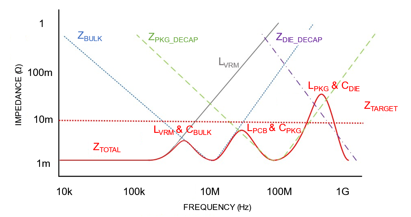
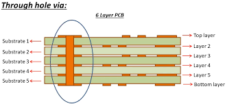
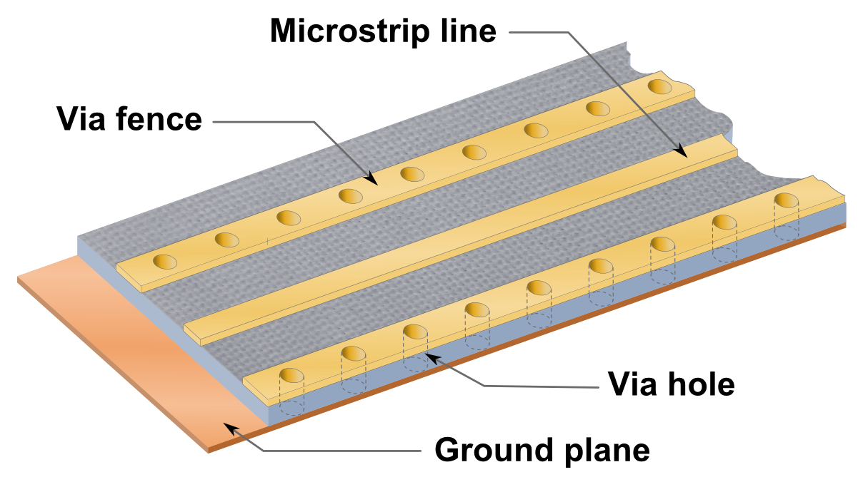
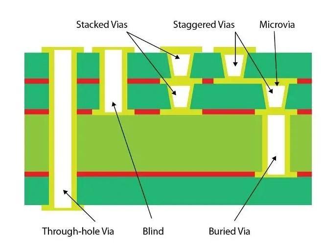
PCB stack up and via design play a key role in maintaining signal integrity in high speed applications. This guide explains how to reduce reflections from via stubs, apply backdrilling, and arrange layers for consistent impedance and reliable performance.