ALLPCB


Creating stunning 3D models of your printed circuit boards (PCBs) is easier than ever with modern PCB design software. Whether you're an engineer, hobbyist, or designer, 3D visualization in PCB design helps you see your project in a realistic way before manufacturing. By using PCB design software with 3D capabilities, you can design, visualize, and even export detailed models for presentations or prototyping. In this guide, we'll walk you through the process of 3D PCB modeling, from choosing the right tools to exporting PCB models for various uses. Let's dive into the steps and tips for creating realistic PCB models that stand out.
Why 3D Visualization in PCB Design Matters
Before we get into the how-to, let’s understand why 3D visualization in PCB design is so important. Traditional 2D layouts give you a flat view of your board, but they often fail to show how components fit together in real space. A 3D model lets you spot potential issues like component interference, enclosure fitment problems, or heat dissipation challenges early in the design process. This can save you time and money by reducing errors before production.
Moreover, 3D models are perfect for sharing your ideas with clients or team members. A realistic visual representation can communicate complex designs more effectively than a 2D schematic. Plus, many industries now expect 3D models as part of the design process for integration with mechanical CAD tools. With the rise of compact and intricate electronics, mastering 3D PCB modeling is a must-have skill.
Choosing the Right PCB Design Software with 3D Capabilities
The first step in creating stunning 3D models is selecting the right PCB design software with 3D features. Not all tools offer robust 3D visualization, so it’s important to pick one that meets your needs. Look for software that supports native 3D modeling, allows realistic rendering of components, and offers options for exporting PCB models in common formats like STEP or IGES.
Key features to consider include:
- Native 3D View: The ability to toggle between 2D and 3D views seamlessly.
- Component Library with 3D Models: A built-in library of components with accurate 3D representations.
- Export Options: Support for exporting 3D models to integrate with mechanical design tools or for sharing.
- Realistic Rendering: Tools for adding textures and colors to make your PCB look lifelike.
By choosing software with these features, you’ll have a strong foundation for creating realistic PCB models. Many modern tools also provide tutorials and community support to help you get started with 3D visualization.
Step-by-Step Guide to Creating Realistic PCB Models
Now that you’ve chosen your software, let’s walk through the process of 3D PCB modeling. These steps are general and can apply to most design tools with 3D capabilities. We’ll focus on practical actions to help you achieve stunning results.
Step 1: Design Your PCB Layout in 2D
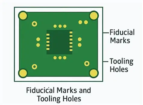
Every 3D model starts with a solid 2D layout. Begin by creating your schematic and placing components on the board. Pay attention to details like trace widths (e.g., 0.2 mm for high-speed signals) and spacing to meet impedance requirements (such as 50 ohms for RF designs). A well-designed 2D layout ensures that your 3D model will be accurate and functional.
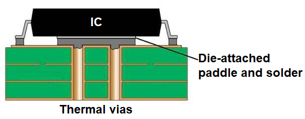
During this stage, double-check your component placement for potential physical conflicts. For example, ensure tall components like electrolytic capacitors (often 10-15 mm in height) don’t overlap with connectors or other parts. This groundwork is critical for a smooth transition to 3D visualization.
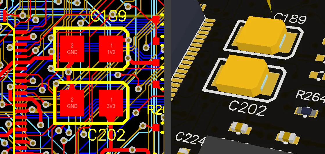
Step 2: Assign 3D Models to Components
Most PCB design software with 3D features includes a library of pre-built 3D component models. For each part in your layout, assign the corresponding 3D model. If a specific component isn’t available in the library, you may need to download or create a custom 3D model using external tools or built-in editors.
For accuracy, ensure the dimensions match real-world specs. For instance, a standard 0805 resistor should measure approximately 2.0 mm x 1.25 mm x 0.5 mm. This attention to detail is what makes creating realistic PCB models possible. Some tools also allow you to adjust the color and texture of components for a more polished look.
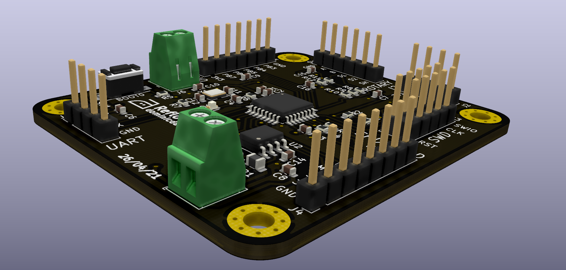
Step 3: Switch to 3D View and Refine the Model
Once all components have 3D models assigned, switch to the 3D view in your software. This mode lets you see your board from different angles, often with options to rotate, zoom, and pan. Check for any misalignments or errors, such as components floating above the board or incorrect heights.
Refine the model by adjusting component positions if needed. Some tools allow you to add realistic details like solder joints or silkscreen text for a more professional appearance. If your software supports it, apply textures to the board substrate (e.g., a green solder mask) and metallic finishes to traces for enhanced realism.
Step 4: Verify Mechanical Integration
One of the biggest advantages of 3D visualization in PCB design is the ability to check how your board fits into its enclosure or alongside other hardware. Import your PCB model into a mechanical design tool or use built-in integration features to test for clearance issues. For example, ensure there’s at least 2 mm of space between the tallest component and the enclosure lid to avoid physical contact.
This step is especially important for compact designs like wearable devices, where every millimeter counts. Identifying fitment issues at this stage can prevent costly redesigns later.
Step 5: Exporting PCB Models for Sharing or Manufacturing
After finalizing your 3D model, you may need to export it for various purposes, such as client presentations, 3D printing, or integration with other systems. Most PCB design software with 3D capabilities supports exporting PCB models in formats like STEP, IGES, or STL. Choose the format that best suits your needs—STEP is often used for mechanical CAD integration, while STL is common for 3D printing.
Before exporting, check the file for errors or missing elements. Some tools provide a preview of the exported model to ensure all details are intact. If you’re sharing the model with a manufacturing partner, include annotations or documentation to clarify critical dimensions or features.
Tips for Enhancing Your 3D PCB Models
Beyond the basics, here are some tips to take your 3D PCB modeling to the next level and create truly stunning visuals:
- Use High-Quality Component Models: Invest time in sourcing or creating detailed 3D models for components. Accurate representations of items like ICs with pin details or connectors with locking mechanisms can make a big difference.
- Add Environmental Context: Some software lets you place your PCB in a virtual enclosure or alongside other parts for a more complete visualization. This is great for presentations.
- Experiment with Lighting and Shadows: If your tool supports rendering options, play with lighting effects to highlight specific areas of your board. Realistic shadows can add depth to your model.
- Optimize File Size: When exporting PCB models, balance detail with file size. Highly detailed models can slow down systems or cause compatibility issues. Simplify where possible without losing critical information.
Common Challenges in 3D PCB Modeling and How to Overcome Them
While 3D visualization in PCB design is powerful, it’s not without challenges. Here are a few common issues and solutions:
Challenge 1: Missing or Inaccurate 3D Models
Solution: If a component lacks a 3D model in your software’s library, search online repositories or manufacturer websites for compatible files. Alternatively, use basic shapes to approximate the part’s dimensions as a placeholder until a detailed model is available.
Challenge 2: Software Performance Issues
Solution: Rendering detailed 3D models can strain your computer’s resources, especially for complex boards. Reduce the level of detail in the display settings or work on smaller sections of the board at a time to improve performance.
Challenge 3: Integration with Mechanical Design
Solution: If your exported model doesn’t align with mechanical designs, double-check the export settings and coordinate systems. Ensure both tools use the same units (e.g., millimeters) and origin points for accurate alignment.
Benefits of Mastering 3D Visualization in PCB Design
Investing time in learning 3D PCB modeling offers numerous benefits for engineers and designers. First, it improves design accuracy by allowing you to spot errors that might be invisible in 2D views. For instance, ensuring a heat sink with a height of 25 mm doesn’t clash with nearby components can prevent thermal issues down the line.
Second, 3D models enhance collaboration. Sharing a realistic visual with stakeholders or manufacturers reduces misunderstandings and speeds up approval processes. Finally, it gives you a competitive edge—clients and employers value professionals who can deliver polished, modern designs using the latest tools.
Conclusion: Elevate Your PCB Designs with 3D Modeling
Creating stunning 3D models of your PCBs is a game-changer in electronics design. By leveraging PCB design software with 3D capabilities, you can visualize your boards in detail, catch potential issues early, and present your work in a professional way. From designing in 2D to exporting PCB models for manufacturing or sharing, each step of 3D PCB modeling adds value to your projects.
Start by selecting the right software, follow the step-by-step process, and apply the tips shared in this guide to create realistic PCB models. With practice, you’ll be able to produce visuals that not only look impressive but also improve the quality of your designs. Embrace 3D visualization in PCB design today and take your skills to the next level with tools and techniques that make your boards stand out.