PCB Specifications
| Category | Capability | Details | Graphical description |
|---|---|---|---|
| Layers | 1-32 | The number of layers refers to the number of electrical layers in the PCB (the number of copper layers) | - |
| Laminated Structure | 4 layers, 6 layers, 8 layers, 10 layers | The laminated structure shown is the common structure recommended by our company | ALLPCB Standard Stack Up |
| Material Type | FR-4 |
Shengyi: Tg140/150/170
Kingboard: Tg130/150 Goldenmax: Tg130 |
Kingboard-Tg150.pdf
Goldenmax-Tg130.pdf Kingboard-Tg130.pdf Shengyi-Tg140.pdf Shengyi-Tg150.pdf Shengyi-Tg170.pdf |
| High Frequency Board | Rogers | Rogers.pdf | |
| CEM-1 | Kingboard: Tg130 | Kingboard-Tg130 | |
| Aluminum | Goldenmax: Tg130 | Goldenmax-Tg130 | |
| Thermoelectric Separation Copper Substrate | Jinpin Technology Copper Plate | - | |
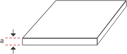
| Dimensions | Maximum size | Standard: a:630×b:520mm |

|
| Minimum size | 1. The minimum production size of a single PCB is 10×5mm 2. The minimum production size of an panel PCB is 50×50mm 3. A single PCB size below ≤ 20×20mm is an ultra-small board | ||
| Board thickness range | 2 layers: 0.4-4.0mm 4 layers: 0.4-4.0mm 6 layers: 0.6-4.0mm 8 layers: 1.0-4.0mm 10 layers: 1.0-4.0mm |
|
|
| Board thickness tolerance | T≥1.0mm:±10% T<1.0mm:±0.1mm | - | |
| Inner layer/outer layer copper thickness | Inner layer: 1oz, 2oz, 3oz, 4oz, 5oz, 6oz Outer layer: 1oz, 2oz, 3oz, 4oz, 5oz, 6oz |
Also known as copper weight
35μm=1oz, 70μm=2oz, 105μm=3oz |
- |
| Imaging production | Negative film, pattern electroplating (traditional tin plating positive film process) | - | |
| Surface treatment | Bare Copper, OSP, HASL With Lead, HASL Lead-free, Immersion Gold, Immersion Tin, Immersion Silver, Nickel Palladium Gold, OSP+ Selective Immersion Gold, Lead-free HASL + Selective Immersion Gold, Lead-free HASL + Selective Gold Plating | - | |
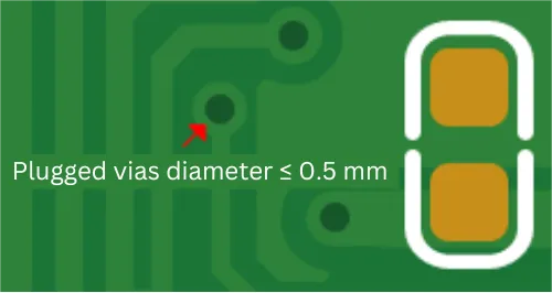
| Plugged vias | Use soldermask ink | ① Only the vias covered with soldermask ink on double sided can be made ② Vias edge to opening pad edge≤0.2 are difficult to make plugged vias ③ Vias diameter≤0.5mm |
|
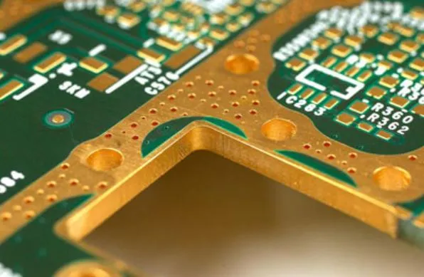
| Metal edging process | Metal edging copper thickness ≥ 15um |
|
|
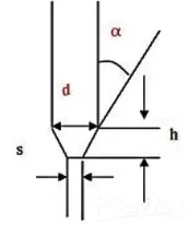
| Gold finger beveling | PCB thickness: 0.8-2.4mm PCB size: Min 50*80mm Max: 500*200mm Angle: 10-70° Angle tolerance: ±5° Depth tolerance: ±0.15mm |
|
|
| Electrical test | Flying probe test: unlimited Test rack≤3500 points | - | |
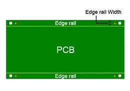
| Edge rail | ≥4mm |
|
|
| FQC | Warpage degree: 0.75% | - |
Drilling & Hole
| Category | Capability | Details | Graphical description |
|---|---|---|---|
| Drilling | Drill Hole Size | 0.15~6.5mm | |
| Rate of finished board thickness to min plated hole diameter | 10:1 |
|
|
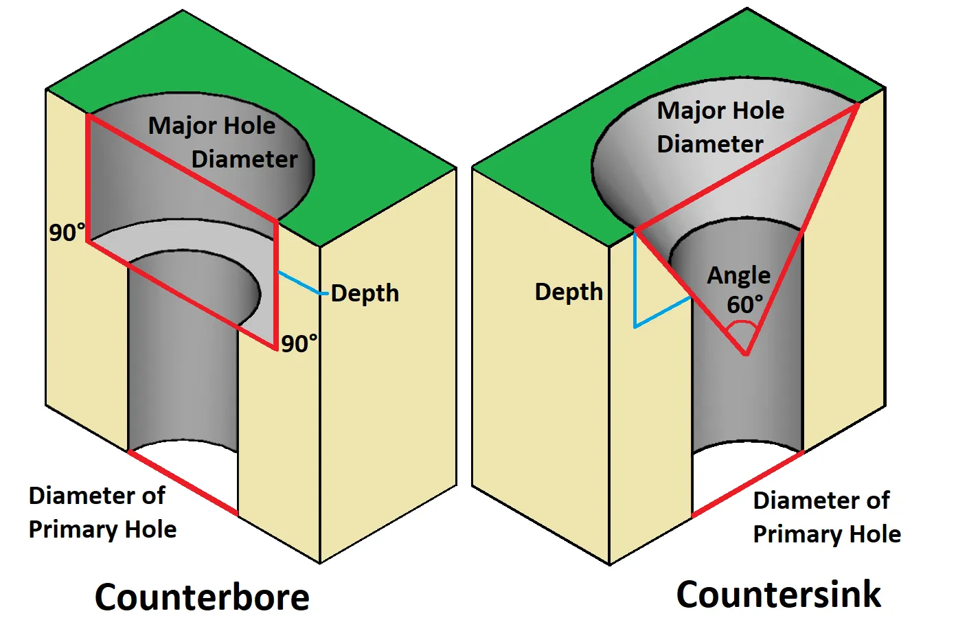
| Countersink hole | 1. Hole size specification: <6.5mm 2. Angle: 90° 140° 180° 3. Hole size tolerance: ±0.1mm 4. Depth Tolerance: ±0.15mm |
|
|
| Drill Hole Size Tolerance | 1. Diameter of plug-in hole: +/-0.075mm 2. Diameter of crimping hole: +/-0.05mm (leave note when order) | - | |
| Minimum Via/Pad | Double-side board: 0.2mm (inner diameter)/0.5mm (outer diameter) Multi-layer board: 0.15mm (inner diameter)/0.25mm (outer diameter) ①The outer diameter must be 0.1mm larger than the inner diameter, 0.15mm preferred ②Preferred Min. Via hole size: 0.2mm |

|
|
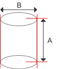
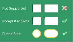
| Min. Plated Slot | Width≥0.7mm |

|
|
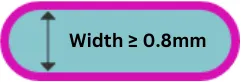
| Min. Non-Plated Slots | Width≥0.8mm |
|
|
| Rectangle Hole/Slot | Don't support |
|
|
| Plated Hole Copper Thickness | 18-100um | - | |
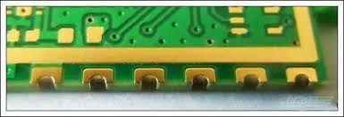
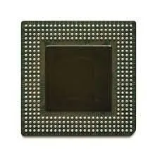
| Plated Half Hole | When it comes to plated half hole, it also called castellated holes, which is plated with copper based on the specialized process on the edge of PCB. And plated half-holes are predominantly used for board-on-board connections, mostly where two boards with different technologies are combined. E.g. the combination of complex microcontroler modules with common, individually designed PCBs ① Diameter: ≧0.4mm ② Spacing: ≥0.35mm ③ Pad edge to board edge: ≧1MM ④ Min. board size: 10*10mm |
|
Minimum trace width and spacing
| Category | Capability | Details | Graphical description |
|---|---|---|---|
| Trace | Min. trace width/spacing (1OZ) | 0.076/0.076mm(3mil/3mil) |
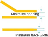
|
| Min. trace width/spacing (2OZ) | 0.14/0.14mm (5.5mil/5.5mil) | ||
| Min. trace width/spacing (3OZ) | 0.2/0.2mm (8mil/8mil) | ||
| Min. trace width/spacing (4OZ) | 0.25/0.25mm (10mil/10mil) | ||
| Min. trace width/spacing (5OZ) | 0.35/0.35mm (14mil/14mil) | ||
| Min. trace width/spacing (6OZ) | 0.45/0.45mm (18mil/18mil) | ||
| Trace Width Tolerance | ±20% | - | |
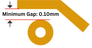
| Pad Edge to trace Edge Spacing | ≧0.1mm (greater if possible), BGA pad to trace minimum spacing 0.075mm |
|
|
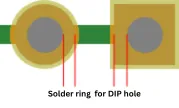
| Width of solder ring for plated DIP holes(1OZ) | ≧0.2mm (recommended value), the limit value is 0.18mm | - | |
| Width of solder ring for non-plated DIP holes | ≧0.4mm (recommended value), because the dry film is used to seal the hole, and the 0.15MM pad or copper surface will be hollowed out around the copper-free hole . Please try to increase the pad for soldering If the pad is too small, it may be a coil or no pad |
|
|
| BGA | ① BGA pad diameter: ≧0.2mm ② BGA pad edge to trace edge: ≧0.075mm |
|
Silkscreen
| Category | Capability | Details | Graphical description |
|---|---|---|---|
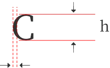
| Silkscreen | Text height | h≧0.75mm, character width 0.1mm (special font, Chinese, hollow character height h>38mil (0.97mm)) |
|
| Text width | ≧0.1mm (lower than this value may not be printed) | ||
| Spacing from character to exposed copper pads | ≧0.15mm (lower than this value will hollow out the characters to avoid contacting the pad) |
Solder Mask
| Category | Capability | Details | Graphical description |
|---|---|---|---|
| Solder Mask | Solder Mask Color | Green, Cold White, Blue, Black, Yellow, Red, Purple, Matte Black, Matte Green | - |
| Solder Mask Thickness | ≧10um |

|
|
| Minimum Solder Bridge Width | 1. Green: 0.075mm 2. Other colors: 0.125mm (red, yellow, blue, white, matte green, black, matte black, purple) |

|
Panelization
| Category | Capability | Details | Graphical description |
|---|---|---|---|
| Panelization | Profiling | edge forming | 1. Forming edge to forming edge A: ±0.15mm; |
| V-cut | Angle: 25°, 30° According to different plate thickness: Remaining thickness: 0.25-0.8mm Remaining thickness tolerance: ±0.1mm | ||
| Maximum size of V-CUT | 1000*1500mm | ||
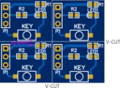
| Panel by V-cut | ① The distance between the V-cut line and the copper ≧0.4mm ②The default is to use 0-gap paneling (only two sides of the V-cutting are required, and the other two sides can use a panel gap of 1.6mm or 2mm) |
|
|
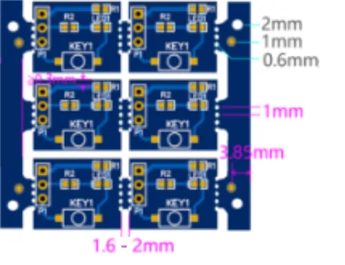
| Panel by stamp holes | ① The distance between the copper and the edge of the board at the non-stamp hole is ≧0.3mm ② Tolerance of the gong edge at the non-stamp hole: ±0.2mm (common gong), ±0.1mm (premium gong) ③ The default board gap is 1.6mm or 2mm ④There will be a gear shape at stamp hole position after the panel is separated. ⑤ Minimum width of edges rails is 4MM (our SMT requires 5mm width, 1mm for fiducial mark, 2mm for tooling hole, 3.85mm from fiducial mark to board edge). |
|