What is Via in PCB?
In the world of printed circuit boards, the term via refers to a hole that is drilled into the PCB to allow electrical connections between different layers. These vias are essential for multi-layer PCBs, enabling signals, power, and ground connections to pass through the various layers of the board. Vias play a crucial role in the functionality and performance of a PCB, and understanding their types, processes, and functions is key to successful PCB design and manufacturing.
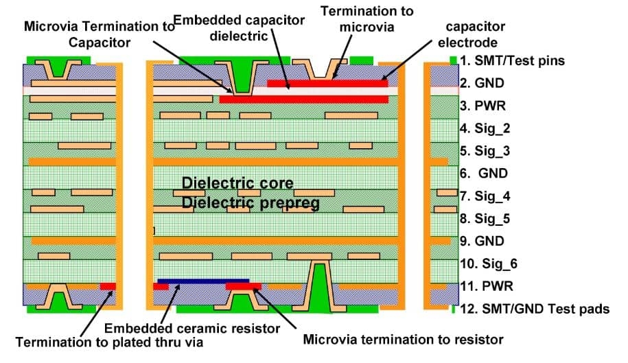
Vias are tiny conductive paths that establish electrical connections between different PCB layers. Depending on their functionality, vias are classified as through-hole, blind, buried, and micro-vias. Microvias are further divided into stacked and staggered vias.
A via consists of a barrel, a pad, and an anti-pad. A barrel is a conductive tube that fills the drilled hole and a pad connects each end of the barrel to the component, plane, or trace. Antipad is a clearance hole between the barrel and the no-connect metal layer.
In the article below, we will introduce the different types of PCB vias, via-in-pad technology, via processes, and factors affecting via design.
Types of Vias
There are several types of vias used in PCB design, each with different applications based on the specific needs of the design. The most common types of vias are:
Through-Hole Via
Definition: These are the most traditional and widely used vias. Through-hole vias go all the way through the PCB, connecting the top and bottom layers.
Applications: These are used when an electrical connection is required between the outer layers of a multi-layer PCB.
Advantages: Cost-effective and easy to fabricate.
Limitations: This can take up more space and increase the board’s overall thickness.
Suggested Reading:Mastering Through-Hole Vias: A Comprehensive Guide to PCB Layer Connections
Blind Vias
Definition: Blind vias connect an outer layer to one or more inner layers of the PCB, but they do not go all the way through the board.
Applications: Often used in high-density designs where space is limited, but connections need to be made between the outer layers and internal layers.
Advantages: Saves space and maintains the integrity of the PCB.
Limitations: More complex to fabricate and often more expensive.
Suggested Reading:Mastering Blind Vias: A Comprehensive Guide for PCB Designers
Buried Vias
Definition: Buried vias connect two or more inner layers, but they do not reach the outer layers of the PCB.
Applications: Used in complex multi-layer designs where inner layers need to be interconnected without affecting the outer layers.
Advantages: Reduces the space occupied by vias on the outer layers, optimizing space for component placement.
Limitations: More expensive and difficult to manufacture due to the need for precise drilling and layer alignment.
Micro Vias
Definition: Micro vias are extremely small holes, typically less than 0.2mm in diameter. These are used in high-density interconnect HDI PCBs to make connections between microelectronic components. Microvias are further divided into stacked and staggered vias.
Applications: Found in advanced, high-performance devices like smartphones, tablets, and high-speed circuits.
Advantages: Saves space and supports high-density designs.
Limitations: Expensive and require advanced manufacturing processes.
Via in pad
The least common type of PCB vias is the via in pad. Only big PCB pads such as the pads of MOSFET and BGA can be drilled with holes, and the holes on big PCB pads are vias-in-pad, which are used for thermal dissipation of the components.
Whether or not to design the via-in-pad? It all depends on the actual situation, and you need to know its pros and cons.
Pros: a via-in-pad provides convenience for routing and avoids parasitic inductance of vias.
Cons: during reflow soldering, solder paste may flow through the via, and it causes poor soldering on the PCB pad.
ALLPCB has rich experience in SMT assembly for vias-in-pad. If you have designed a vias-in-pad, you can contact our representative before production. In most cases, we suggest you make resin plug holes and capped surface treatment to prevent potential drawbacks.
Suggested Reading:Via-in-Pad Microvias: Maximizing Density and Performance in BGA Designs
Via Processes
The process of creating vias in a PCB involves several steps:
-
Drilling: The first step is to drill holes into the PCB. Depending on the type of via being used, the drill may go all the way through the board (for through-hole vias) or stop at a specific layer (for blind or buried vias).
-
Copper Plating: After the holes are drilled, the vias are plated with copper. This step ensures that the vias can conduct electricity and create the necessary electrical connections between layers. Copper plating is typically done through an electrolytic plating process.
-
Via Filling (Optional): In some cases, vias are filled with conductive or non-conductive materials. This is often done to improve signal integrity, especially in high-frequency designs, or to prevent issues like solder wicking. Non-conductive filling material may also be used in designs where vias are not intended to carry current.
-
Via Sealing: After the via is filled and plated, it is sealed with a protective layer to prevent moisture or contaminants from entering the via and causing reliability issues. This is important in ensuring the longevity and performance of the PCB.
This is just a brief overview. We will have a more detailed article later to introduce the relevant knowledge.
How to Determine the Right Via Requirements for Your PCB
It’s important that you and Allpcb select the right via for your project – and that you understand design for manufacturability. Here are 5 factors to consider as you think about your next project:
Via type
What would be best for your project: a buried, blind, or through via? If you have one lamination with no via fill or technology you will have a lot of room for larger holes.
Via size
The most common via size is 10 mil, which would be 7 mil after plating, but via size depends on the thickness of the board. It’s an aspect ratio equation. Micro vias, both laser drilled and mechanically drilled 4 mil holes, are related to the thickness of the boards.
Via tolerance
It’s important to specify hole size tolerance, For Allpcb, we generally only have negative tolerance, and the tolerance value is around -10%.
Support the appropriate technology
When you need blind or buried vias, consult with ALLPCB to begin developing a stack-up that supports that technology.
IPC guidelines
It’s essential to always follow IPC guidelines for the associated technology, which include stipulations such as distance between vias. IPC design guidelines for Class 2, Class 3, Class 3DS, and military are especially important because they all differ slightly.
 ALLPCB


