 ALLPCB


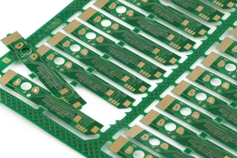
Depanelization is the separation of individual circuit boards from the PCB panel or array. The depanelization method of printed circuit boards (PCBs) directly affects production efficiency and product quality. Stamp hole and V-cut (V-scoring) are two common depanelization technologies. Let's discuss with ALLPCB about the depanelization method of stamp hole connection in detail, analyze its advantages and disadvantages, and compare it with the V-scoring depanelization method to explore its practicality and performance in actual operation.
What is stamp hole?
Stamp hole is a method of drilling small holes on the predetermined dividing line of the circuit board so that the boards remain connected during the production process and are finally separated by simple breaking or cutting with a separation machine. This method is similar to the jagged holes on the edge of a stamp, hence the name stamp hole, also called mouse bites hole.
Design suggestions
The design specifications of stamp holes usually include hole diameter, hole spacing, and the distance between the hole and the edge of the pcb printed circuit board. Common design specifications are as follows:
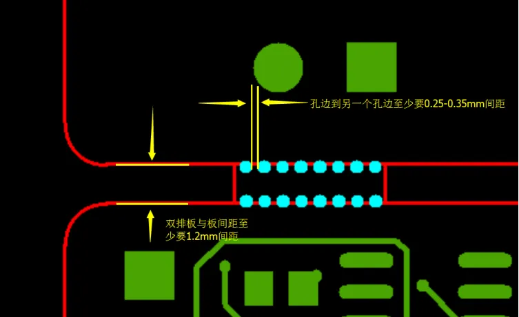
Hole diameter: usually between 0.6 mm and 1.0 mm. Smaller hole diameters (such as 0.6 mm) are suitable for boards that require higher precision and strength, while larger hole diameters (such as 1.0 mm) facilitate easier separation operations.
Hole spacing: The distance between holes is usually 1.0 mm to 1.5 mm. This distance can be adjusted according to the thickness of the PCB and the required strength. A denser hole spacing (such as 1.0 mm) is suitable for thinner boards, while a sparser spacing (such as 1.5 mm) is suitable for thicker boards.
Distance between holes and board edges: Usually maintained between 0.2 mm and 0.5 mm. This distance must ensure the strength of the board and facilitate subsequent board separation operations.
For more on selecting the right method for your board layout, see Depaneling Demystified: Choosing the Right Method for Your PCB Panel Size
Advantages of stamp hole board connection
Easy processing: The stamp hole board connection method only requires additional drilling steps during PCB manufacturing, and the operation is relatively simple and easy to implement.
Low cost: Since no special equipment is required during the processing of the stamp hole board connection, only some process steps are added during the drilling stage, so the cost is relatively low.
Reduce stress: This method has less stress during board separation, which is particularly suitable for PCBs that need to protect sensitive components and precision circuits.
High flexibility: The position and number of stamp holes can be flexibly adjusted according to actual needs, and is suitable for PCB designs of various shapes and sizes.
Tab Routing: Balanced Between Precision and Flexibility
Tab routing combines CNC routing of PCB outlines with small tab bridges, often reinforced by mouse bites. This allows for flexible board shapes while providing strong support during handling.
-
Precise edge routing for complex contours
-
Tabs are removed post-assembly, usually with pliers or a punch
-
Reduced edge stress compared to full routing or V-scoring
Get hands-on advice in Mastering Tab Routing: Techniques for Clean and Stress-Free PCB Depaneling
Laser Depaneling: Precision for High-Density Boards
Laser depaneling uses UV or CO? lasers to cut or ablate material. This method is ideal for high-density interconnect (HDI) and flexible PCBs due to its ultra-low mechanical stress.
Benefits
-
Non-contact cutting
-
Ideal for microfeatures and tight tolerances
-
No burrs, no delamination
-
Automated and programmable
Challenges
-
High upfront cost of laser equipment
-
Slower cutting speeds for thicker substrates
Explore capabilities in Laser PCB Depaneling: Achieving High Precision and Minimal HAZ
Automated vs Manual Depaneling
Automated systems reduce operator error, increase repeatability, and are essential for high-volume environments. Manual depaneling, while lower in cost, may not meet IPC standards for high-reliability sectors.
Understand both strategies in Automated Depaneling vs. Manual Breakaway: Which Method is Right for You?
Choosing the Right Depaneling Method
| Method | Cost | Edge Quality | Stress | Best Use Case |
|---|---|---|---|---|
| Stamp Hole | Low | Rough | Low | Prototyping, flexible designs |
| V-Scoring | Medium | Smooth | High | Mass production |
| Tab Routing | Medium | Clean | Low | Custom shapes, mid-volume |
| Laser Cutting | High | Excellent | None | HDI, sensitive components |
| Manual Break | Low | Rough | High | Low-volume, non-critical apps |
Further optimize your workflow with Optimizing PCB Depaneling: A Comprehensive Guide to Methods and Best Practices
What is a V-scoring?
V-Cut is a common PCB depaneling method with two main advantages: first, V-Cut can provide smoother and more consistent board edges; second, V-Cut has advantages in material utilization, especially for large-volume or high-layer boards, where every square inch of material is important, so it can bring significant cost savings.
V-Cut Cutting Specifications and Design Suggestions
Panel Boundary: It is recommended to use a substrate of at least 5.00 mm as the panel boundary. Add two parallel edges on the two longest sides of the PCB, and leave no gaps between the boards. The V-Cut will be processed along the shared board outline.
Processing Direction: V-Cut is processed only along the x-axis and y-axis directions, and no diagonal processing is performed. Because the V-Cut will run through the entire board along the array straight line, the board outline should be straight.
Scoring Depth: The scoring depth is about one-third of the total material thickness. The scoring line will be processed on the upper and lower sides of the PCB, leaving a material thickness of about one-third of the total thickness. For example, if the board thickness is 0.062 inches, the remaining material thickness will be about 0.021 inches.
Board Thickness Requirements: It is recommended to use V-scoring technology only on panels with a minimum board thickness of 1 mm to ensure stability. However, in practice, the thickness of the inner mesh material of the V-scoring can vary from 0.15 mm to 0.4 mm depending on the length of the scoring. If the scoring length is less than 25 mm, the mesh thickness can be 0.15 mm; scorings with a length of 100 mm can have a mesh thickness of 0.25 mm; scorings longer than 100 mm can have a mesh thickness of 0.4 mm. These values ??are guidelines only and should be discussed with your assembly shop to confirm the mesh thickness for your board design.
Board Material: Standard PCB material is basically fiberglass. Even if the board has a V-scoring, it will still be strong, so be careful when separating the boards. Expect some degree of flexing before the scoring line breaks. It is normal for some fiberglass filaments to appear along the edge of the V-scoring. Light sanding with a belt sander can take care of any rough areas.
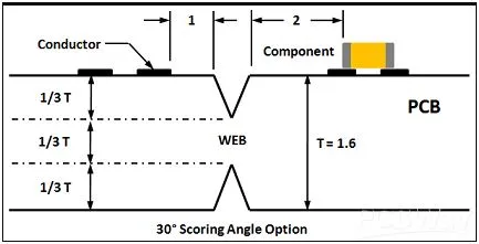
The V-scoring cutting selection is very important. With the difference in drill bit and cutting angle, all wires and circuit boards should be arranged within a range of at least 1 mm from the top of the V-scoring edge to prevent damage during the depaneling process. The middle layer should be pulled back 1 mm from the V-scoring to maintain a ratio of 1/3 in the upper, middle and lower parts.
Advantages of V-scoring
1. Flat edges: The edges of the V-scoring after depaneling are relatively flat, which reduces the subsequent processing steps and improves the product appearance and assembly quality.
2. High production efficiency: The V-scoring is suitable for mass production, and the mechanical operation is simple and fast, which improves production efficiency.
3. Stable structure: Even before depaneling, the overall strength of the circuit board is high, reducing the risk of damage during transportation and assembly.
4. Strong adaptability: Suitable for PCBs of various thicknesses, especially thicker multilayer boards.
What are the differences bewteen V-Scoring or Stamp Hole?
Processing complexity and cost
Stamp hole: simple processing, low cost, suitable for production of all sizes, especially small batches or rapid prototyping.
V-scoring: complex processing, high equipment cost, more suitable for mass production.
Depaneling quality
Stamp hole: uneven edges, need additional trimming, suitable for products that do not require high appearance quality.
V-scoring: flat edges, high quality, suitable for products with high quality requirements.
Depaneling stress
Stamp hole: low stress, suitable for sensitive and precision components.
V-scoring: high stress, need to pay attention to the protection of components.
Design flexibility
Stamp hole: flexible design, can adapt to various shapes and layouts.
V-scoring: limited design, suitable for regular shapes and fixed layouts.
Applicable scenarios
Stamp hole:
Small batch production or single piece production.
Beginners or hobbyists do not have complex equipment.
The board has various shapes and needs to be flexibly adjusted.
The finished product does not require high edge flatness.
Recommended examples:
Small circuit boards such as Arduino expansion boards and sensor modules.
DIY electronic projects, such as simple LED driver boards, audio amplifiers, etc.
V-scoring:
Massive production or high production efficiency.
Hobbyists have the conditions to use special equipment or tools.
The board design is relatively regular and suitable for fixed layouts.
The finished product has high edge flatness requirements.
Suggested Reading: V-Scoring vs. Stamp Hole Depaneling: Choosing the Right Method for Your PCB
Looking Ahead: The Future of PCB Depaneling
As electronic designs grow in complexity and customer expectations increase, the future of depaneling lies in automation, precision, and eco-efficiency. Innovations such as AI-assisted routing, predictive maintenance of cutting tools, and green manufacturing practices are reshaping how PCB depaneling is performed.
Explore more about the industry's direction in The Future of PCB Depaneling: Emerging Trends and Technologies
Summary
Stamp hole connected boards and V-scoring each have their own advantages and disadvantages. In actual applications, engineers usually consider factors such as custom PCB cost, production efficiency, product quality and design flexibility, and choose the most appropriate board separation method to achieve the best production effect and product performance. Close cooperation with PCB manufacturers should be carried out according to specific project requirements and equipment conditions to ensure the best design and processing results.


