 ALLPCB


The silkscreen layer on a printed circuit board (PCB) is more than just a visual add-on - it's a critical tool for ensuring clarity during assembly, testing, and maintenance. For engineers, a well-designed silkscreen can mean the difference between a seamless production process and costly errors. At its core, PCB silkscreen design involves printing text, symbols, and graphics onto the board's surface to identify components, indicate polarity, and provide essential information. However, achieving legibility while adhering to industry standards is no small feat, especially as boards become smaller and more complex.
In this blog, we'll explore the principles of effective PCB silkscreen design, focusing on legibility, industry standards, and practical tips to optimize your designs. Whether you're a seasoned engineer or new to PCB layout, this guide will equip you with actionable insights to enhance your silkscreen layers.
What Is PCB Silkscreen and Why Does It Matter?
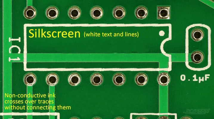
The silkscreen layer, often called the "legend layer," is a non-conductive ink coating applied to the surface of a PCB. It includes markings such as reference designators (e.g., R1 for a resistor), polarity indicators, pin numbers, test points, and regulatory symbols. These markings serve multiple purposes:
- Assembly Guidance: Silkscreen helps technicians identify and place components correctly during PCB assembly.
- Troubleshooting Aid: Clear markings simplify debugging and maintenance by making components and test points easy to locate.
- Regulatory Compliance: Markings like RoHS, CE, or UL symbols ensure the board meets industry standards.
- Branding: Logos and part numbers reinforce manufacturer identity.
Poor silkscreen design - such as illegible text or misplaced markings - can lead to assembly errors, increased PCB manufacturing costs, or even board failure. For instance, a 2017 study by Epec Engineered Technologies noted that clipping of silkscreen data due to poor placement can obscure critical information, potentially causing misinterpretation during assembly.
Key Elements of Silkscreen Design
To create an effective silkscreen layer, engineers must focus on legibility, placement, and compliance with industry standards. Below, we break down the essential elements of silkscreen design.
1. Font Size and Line Width for Legibility
Legibility starts with choosing the right font size and line width. Text that's too small or lines that are too thin can become unreadable, especially during manufacturing or under varying lighting conditions. Industry standards recommend the following:
- Font Size: A minimum of 0.035 inches (0.89 mm) for reference designators, with 0.050 inches (1.27 mm) preferred for optimal readability. Larger fonts (e.g., 0.080 inches) can be used for part numbers or logos.
- Line Width: Use a minimum line width of 0.006 inches (0.15 mm) to ensure the ink prints clearly. For smaller fonts, reduce line width proportionally to avoid ink smudging.
- Font Style: Stick to simple, non-serif fonts like Arial or Helvetica. Complex fonts may distort during printing, reducing legibility.
Example: On a high-density PCB, a reference designator like "C12" should be printed at 0.050 inches with a 0.006-inch line width to ensure clarity for assembly technicians.
Suggested Reading:The Ultimate Guide to Silkscreen Font Sizes for PCB Component Identification
2. Placement and Spacing
Proper placement of silkscreen elements is critical to avoid interference with other PCB features. Overlapping text with pads, vias, or traces can cause manufacturing issues, such as solderability problems or obscured markings. Key guidelines include:
- Clearance: Maintain a minimum clearance of 0.005 inches (0.127 mm) between silkscreen elements and pads, vias, or other objects.
- Avoid Critical Areas: Do not place silkscreen over solder pads, through-hole vias, or high-speed signal lines (e.g., microstrip lines). For high-speed signals, silkscreen ink can alter the dielectric properties, causing impedance discontinuities and signal degradation.
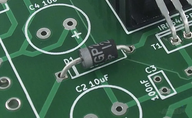
- Proximity to Components: Place reference designators and polarity markers close to their respective components, ensuring they remain visible after assembly. For example, a diode's cathode marker (e.g., a "-" symbol) should be adjacent to the component's cathode pin.
Example: On a multilayer PCB, ensure silkscreen markings for inner-layer components are duplicated on the outer layers to aid identification, as components may be obscured.
3. Orientation and Consistency
Consistent orientation improves readability and reduces confusion during assembly. Follow these best practices:
- Text Direction: Align text to be read from left to right or bottom to top. Limit text rotation to 0° or 90° to avoid forcing technicians to rotate the board repeatedly.
- Component Orientation: Match the silkscreen orientation to the component's datasheet. For instance, an IC's Pin 1 marker should align with the pin's physical orientation to prevent installation errors.
- Uniformity: Use consistent naming conventions (e.g., "R" for resistors, "C" for capacitors) and ensure all components are labeled in the same direction where possible.
4. Color and Contrast
Silkscreen color affects both legibility and manufacturability. The most common silkscreen color is white, as it contrasts well with the standard green solder mask. Other colors like yellow, black, or red are used but may be less manufacturing-friendly. For example, pink silkscreen is discouraged due to its poor adhesion properties.
- Contrast: Choose a silkscreen color that stands out against the solder mask. For a red solder mask, black silkscreen is more visible than white.
- Material: Use non-conductive epoxy ink that resists corrosion and high temperatures to ensure durability during soldering and operation.
Example: A white silkscreen on a green solder mask ensures high visibility, while a black silkscreen on a white solder mask is ideal for aluminum boards to prevent ink peeling.
Suggested Reading:The Ultimate Guide to Silkscreen Contrast on Red Solder Mask PCBs
Industry Standards for PCB Silkscreen Design
Adhering to industry standards ensures that your silkscreen design is compatible with manufacturing processes and meets regulatory requirements. Below are the key standards to follow:
IPC Standards
The Institute of Printed Circuits (IPC) provides guidelines for PCB design, including silkscreen legibility and placement:
- IPC-A-600: Specifies acceptable conditions for PCB markings, including minimum legibility requirements. For example, text must remain readable after manufacturing processes like soldering.
- IPC-2221: Recommends minimum clearances between silkscreen and conductive features to prevent manufacturing defects.
- IPC-7351: Defines standard component footprints, including silkscreen markings for polarity and pin indicators.
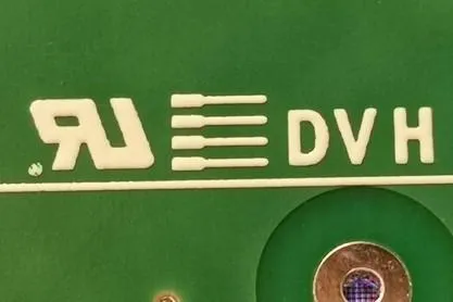
Regulatory Markings
Certain industries require specific silkscreen markings for compliance:
- RoHS: Indicates lead-free components, often marked with a "Pb-free" symbol.
- UL 796/94: Used for safety-certified boards, requiring a UL logo from a certified manufacturer.
- CE/FCC: Common in consumer electronics to denote compliance with European or U.S. regulations.
Example: A medical device PCB may require a RoHS symbol and a UL logo, both printed at 0.050 inches to ensure legibility during inspection.
Common Silkscreen Printing Methods
The method used to apply silkscreen affects its precision and legibility. Here are the three primary techniques:
- Manual Screen Printing: Ink is applied through a mesh stencil. It's cost-effective for low-volume production but limited to a resolution of 0.007 inches (0.18 mm), making it less suitable for dense designs.
- Liquid Photo Imaging (LPI): Uses photosensitive ink exposed to UV light through a photomask. LPI offers higher resolution (down to 0.004 inches) and is ideal for complex designs.
- Direct Legend Printing (DLP): Inkjet printers apply ink directly to the PCB, providing the highest precision for fine text and intricate graphics. DLP is preferred for high-density boards.
Example: For a compact IoT device PCB, DLP ensures that 0.035-inch reference designators remain sharp and legible, even on a crowded board.
Best Practices for Optimizing Silkscreen Design
To create a silkscreen layer that balances legibility, functionality, and manufacturability, follow these best practices:
- Prioritize Critical Information: On space-constrained boards, prioritize regulatory symbols, polarity markers, and reference designators over non-essential markings like logos.
- Test for Clarity: Print the PCB layout at actual size and review it under different lighting conditions. Seek feedback from colleagues to ensure readability.
- Consult Manufacturers: Before finalizing your design, confirm your manufacturer's silkscreen capabilities, such as minimum line width or supported colors.
- Use EDA Software: Tools like Altium Designer or Cadence Allegro offer auto-silkscreen features that adjust text placement to avoid overlaps and ensure compliance with standards.
- Mirror Bottom Layers: For bottom-side silkscreen, ensure markings are mirrored in Gerber files to appear correctly when viewed.
How ALLPCB Supports Your Silkscreen Design Needs
At ALLPCB, we understand the importance of precise and legible silkscreen layers in PCB manufacturing. Our advanced manufacturing facilities and quick-turn prototyping services ensure that your silkscreen designs are accurately reproduced, even for high-density boards. With global logistics and a team of experts, we provide tailored support to help engineers meet industry standards like IPC and RoHS.
Conclusion
A well-designed PCB silkscreen layer is a cornerstone of efficient manufacturing and reliable performance. By focusing on legibility - through proper font sizes, clear placement, and high-contrast colors - and adhering to industry standards like IPC and regulatory requirements, engineers can create boards that are easy to assemble, test, and maintain. As PCBs become more compact and complex, mastering silkscreen design is more critical than ever.
By following the guidelines and best practices outlined in this blog, you can optimize your silkscreen layers for clarity and compliance. Consult with your manufacturer early, leverage professional design tools, and prioritize critical information to ensure your PCBs perform flawlessly in the field.


