 ALLPCB


If you're looking for a quick answer on the best silkscreen font sizes for PCB component identification, here it is: For optimal legibility, aim for a font height of at least 0.040 inches (40 mils or 1.016 mm) with a stroke width of 0.006 inches (6 mils or 0.152 mm). These dimensions ensure clarity for assembly and troubleshooting, even in compact designs. Now, let’s dive deeper into the details of choosing the right font size, understanding legibility factors, and following best practices for PCB assembly silkscreen in this comprehensive guide.
Introduction to PCB Silkscreen and Its Importance
Printed Circuit Boards (PCBs) are the backbone of modern electronics, and every tiny detail on a board plays a crucial role in its functionality and assembly. One such detail is the silkscreen layer, a non-conductive ink applied to the surface of a PCB. This layer includes text and symbols like reference designators, polarity markers, and assembly instructions, making it easier to identify components and assemble the board correctly.
Choosing the right silkscreen font size is vital for ensuring that these markings are readable during assembly, inspection, and repair. A font that's too small can lead to errors, while one that's too large can clutter the board and interfere with component placement. In this guide, we'll explore the best practices for silkscreen font sizes, focusing on component identification and legibility for PCB assembly.
Why Silkscreen Font Size Matters for Component Identification
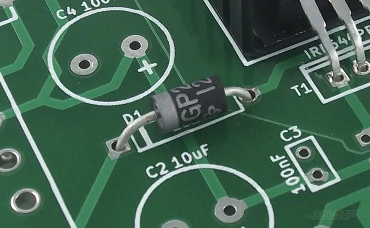
The silkscreen layer serves as a map for engineers, technicians, and assemblers. It labels components with reference designators (like R1 for a resistor or C3 for a capacitor), indicates polarity for diodes and capacitors, and sometimes includes test points or version numbers. If the font size is too small, these markings become unreadable, leading to mistakes during assembly or troubleshooting.
For instance, imagine an assembler misplacing a component because they couldn’t read the tiny reference designator. Such errors can delay production or, worse, cause functional failures in the final product. On the other hand, overly large fonts can crowd the board, especially in high-density designs, making the layout messy and confusing.
Striking the right balance with font size ensures that the silkscreen serves its purpose without compromising the board’s design. Let’s break down the key factors that influence silkscreen legibility on PCBs.
Factors Affecting Silkscreen Legibility on PCBs
Several elements determine how readable your silkscreen markings will be. Understanding these factors will help you choose the right font size and style for your PCB design.
1. Font Height and Stroke Width
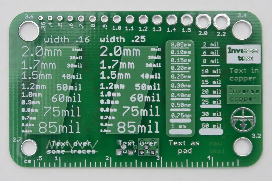
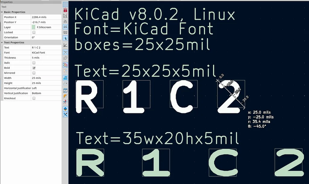
The height of the font and the thickness of its lines (stroke width) are the most critical factors for legibility. A font height of at least 0.040 inches (1.016 mm) is widely recommended as the minimum for readability under normal conditions. The stroke width should be around 0.006 inches (0.152 mm) to ensure the lines are visible without blending together.
2. Board Size and Component Density
On a small or densely populated PCB, space for silkscreen markings is limited. In such cases, you might need to use the minimum recommended font size to fit everything in. For larger boards with fewer components, you can afford slightly larger fonts (up to 0.060 inches or 1.524 mm) for better visibility.
3. Viewing Conditions
Assemblers and technicians often work under varying lighting conditions. A font size that looks readable in a well-lit office might be hard to decipher in a dimly lit factory. Smaller fonts can also be challenging to read for individuals with vision impairments, so sticking to the minimum recommended size helps ensure accessibility.
4. Manufacturing Capabilities
Not all PCB manufacturers can produce extremely fine silkscreen details. If the font size or stroke width is too small, the markings might blur or become illegible during the printing process. Always check with your manufacturing partner to confirm their silkscreen resolution limits, which typically range from 0.004 to 0.008 inches (0.102 to 0.203 mm) for stroke width.
Recommended Silkscreen Font Sizes for PCB Assembly
Based on industry standards and practical experience, here are the recommended font sizes for PCB silkscreen markings, particularly for component identification and reference designators.
- Minimum Font Height: 0.040 inches (40 mils or 1.016 mm)
- Minimum Stroke Width: 0.006 inches (6 mils or 0.152 mm)
- Ideal Font Height for High Visibility: 0.050 to 0.060 inches (1.27 to 1.524 mm)
- Maximum Font Height: Avoid exceeding 0.080 inches (2.032 mm) unless space permits, as larger fonts can clutter the board.
These dimensions are derived from guidelines provided by PCB design standards and feedback from assembly professionals. They ensure that reference designators and other markings remain clear during manual and automated assembly processes.
Font Style Recommendations
Beyond size, the style of the font also impacts legibility. Use simple, sans-serif fonts like Arial or Helvetica, as they are easier to read at small sizes compared to serif or decorative fonts. Avoid italicized or overly stylized text, as it can distort when printed on a PCB surface.
Best Practices for PCB Assembly Silkscreen Design
Choosing the right font size is just one part of creating an effective silkscreen layer. Here are some additional best practices to ensure your silkscreen markings aid in component identification and assembly without causing confusion.
1. Prioritize Key Information
Focus on including only essential information in the silkscreen layer. Reference designators (e.g., R1, C2) are a must for component identification. Polarity markers for diodes, LEDs, and capacitors are also critical to prevent assembly errors. If space is tight, skip non-essential elements like logos or lengthy text.
2. Maintain Uniform Orientation
Ensure all text is oriented in the same direction, ideally readable from a single angle (e.g., left to right, top to bottom). This uniformity reduces the need for assemblers to rotate the board repeatedly, speeding up the process and minimizing errors.
3. Avoid Overlapping with Components and Pads
Place silkscreen text away from solder pads, vias, and component bodies. Overlapping text can be obscured after assembly, rendering it useless. Most PCB design software allows you to set clearance rules to prevent such overlaps automatically.
4. Use Contrasting Colors
White silkscreen ink on a dark solder mask (like green or blue) offers the best contrast for readability. If your board uses a light-colored mask, consider black or dark ink. Confirm with your manufacturer which ink colors are available and test for visibility if possible.
5. Test Legibility in Prototypes
Before mass production, order a prototype and inspect the silkscreen markings under different lighting conditions. If the text is hard to read, adjust the font size or stroke width in your design files. This step can save time and cost by catching issues early.
Common Mistakes to Avoid with PCB Silkscreen Font Sizes
Even experienced designers can make errors when setting up silkscreen layers. Here are some common pitfalls to watch out for:
- Using Fonts Below the Minimum Size: Fonts smaller than 0.040 inches (1.016 mm) are often unreadable, especially after manufacturing tolerances are applied.
- Ignoring Manufacturer Guidelines: Some manufacturers have specific limits on silkscreen resolution. Failing to adhere to these can result in blurred or incomplete markings.
- Overloading the Silkscreen Layer: Including too much text or unnecessary details can clutter the board and reduce overall readability.
- Inconsistent Text Orientation: Text placed at random angles forces assemblers to rotate the board, slowing down the process and increasing the risk of errors.
How Silkscreen Font Size Impacts Assembly and Troubleshooting
During PCB assembly, whether manual or automated, silkscreen markings guide the placement of components. A clear reference designator font ensures that each resistor, capacitor, or IC goes in the correct spot. For polarized components, legible polarity markers prevent reverse installation, which could damage the board or render it non-functional.
In troubleshooting, silkscreen markings are equally important. Technicians rely on reference designators to locate specific components on a schematic and test points for diagnostics. If the font size is too small or the text is unclear, identifying the right component becomes a time-consuming challenge, delaying repairs.
For example, consider a board with a faulty capacitor. If the reference designator “C10” is legible at 0.050 inches (1.27 mm), a technician can quickly find it on the schematic and replace it. But if the text is tiny or blurred, they might waste time guessing which capacitor is C10, potentially desoldering the wrong one.
Suggested Reading:The Impact of Silkscreen Font Size on Automated Optical Inspection (AOI)
Adapting Font Sizes for Different PCB Applications
Not all PCBs are created equal, and font size requirements can vary based on the application. Here’s how to adapt silkscreen font sizes for different scenarios:
1. Consumer Electronics
In compact devices like smartphones or wearables, PCB space is extremely limited. Stick to the minimum font height of 0.040 inches (1.016 mm) and prioritize only critical markings like reference designators and polarity indicators.
2. Industrial Equipment
Industrial PCBs often operate in harsh environments and may be handled by technicians wearing gloves or under poor lighting. Use a slightly larger font height of 0.050 to 0.060 inches (1.27 to 1.524 mm) for better visibility.
3. Prototyping and Educational Boards
For prototypes or learning kits, where clarity is more important than space constraints, consider using larger fonts up to 0.080 inches (2.032 mm). This makes it easier for students or engineers to read markings without magnification.
Conclusion: Mastering Silkscreen Font Sizes for Better PCBs
Choosing the right silkscreen font size for PCB component identification is a small but critical detail that can make or break the assembly and maintenance process. By sticking to a minimum font height of 0.040 inches (1.016 mm) and a stroke width of 0.006 inches (0.152 mm), you can ensure legibility without overcrowding your board. Remember to consider factors like board size, component density, and manufacturing capabilities when designing your silkscreen layer.
By following the best practices outlined in this guide—prioritizing key information, maintaining uniform orientation, and testing legibility—you can create PCB designs that are easy to assemble and troubleshoot. Whether you're working on a compact consumer device or a robust industrial system, the right silkscreen font size will streamline production and reduce errors, saving time and cost in the long run.
With this ultimate guide to PCB silkscreen font sizes, you now have the knowledge to enhance component identification and assembly efficiency. Apply these tips to your next project, and watch how a well-designed silkscreen layer transforms the quality of your boards.


