 ALLPCB


If you're designing a 4-layer PCB and struggling with high-density routing, trace impedance control, or differential pair routing, you're in the right place. This guide dives deep into advanced routing techniques for 4-layer PCBs, covering strategies for high-density layouts, impedance management, differential routing, and the use of blind and buried vias. We'll break down complex concepts into practical tips you can apply to your next project, ensuring optimal performance and manufacturability.
Whether you're working on a compact IoT device or a high-speed communication board, mastering these techniques will help you overcome common challenges in 4-layer PCB design. Let's explore how to elevate your routing skills with actionable insights and real-world considerations.
Why 4-Layer PCBs Are Essential for High-Density Designs
4-layer PCBs are a go-to choice for designs that require more complexity than a 2-layer board can handle but don't need the cost of a 6-layer or higher stackup. With two internal layers typically dedicated to power and ground planes, and outer layers for signal routing, 4-layer PCBs offer a balance of performance, space efficiency, and cost. They're ideal for high-density designs where space is limited, and signal integrity is critical.
In high-density applications, such as wearable tech or compact embedded systems, the ability to route more traces in a smaller area is crucial. However, this comes with challenges like crosstalk, impedance mismatches, and via congestion. Advanced routing techniques for 4-layer PCB high-density routing can help you address these issues, ensuring your board performs reliably under demanding conditions.
Suggested Reading: 4 layers PCB: Everything You Need to Know
Key Challenges in 4-Layer PCB High-Density Routing
Before diving into specific 4-layer PCB routing strategies, it's important to understand the hurdles designers face in high-density layouts. These include:
- Space Constraints: With more components packed into a smaller area, routing traces without violating design rules becomes difficult.
- Signal Integrity Issues: High-density layouts increase the risk of crosstalk and electromagnetic interference EMI compliance testing between traces.
- Thermal Management: Closer component placement can lead to heat buildup, affecting performance and reliability.
- Via Congestion: Using vias to transition between layers in a compact design can clutter the board and complicate routing.
By applying advanced routing techniques, you can mitigate these challenges and create a board that meets both functional and manufacturing requirements.
Advanced 4-Layer PCB Routing Strategies for High-Density Layouts
Routing a high-density 4-layer PCB requires a strategic approach to maximize space while maintaining signal quality. Here are some proven 4-layer PCB high-density routing techniques to consider:
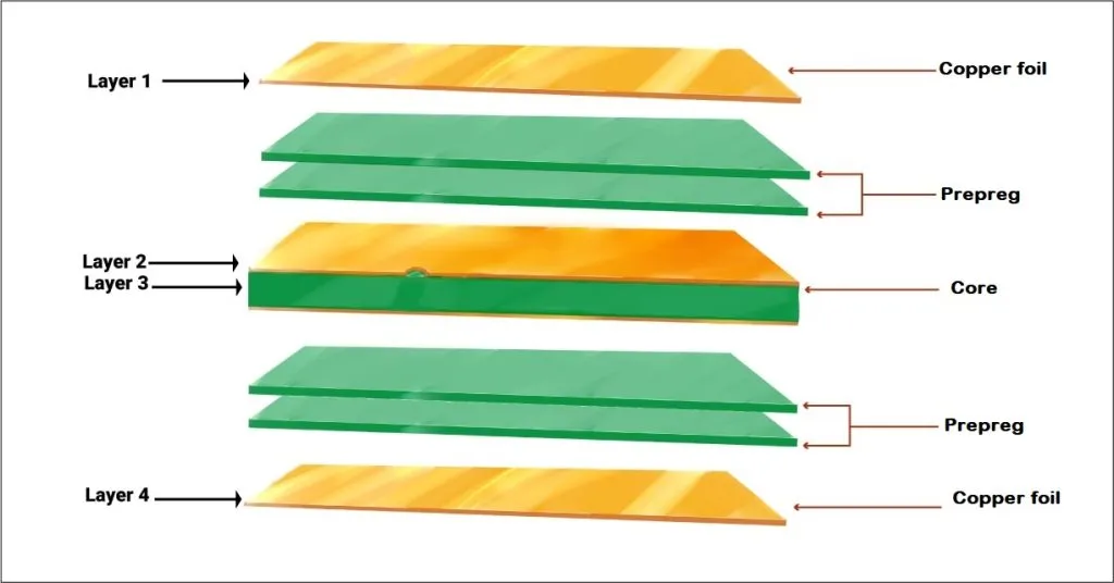
1. Optimize Layer Stackup for Signal and Power Integrity
The typical 4-layer PCB stackup includes two signal layers on the outside and two internal layers for power and ground. This configuration helps reduce EMI by providing a solid reference plane for signals. However, in high-density designs, you might need to dedicate portions of the internal layers for additional routing if space on the outer layers runs out.
For example, reserve the top layer for high-speed signals and critical components, while using the bottom layer for less critical traces. Place power and ground planes on the inner layers to minimize loop inductance, which can be as low as 1-2 nH with proper plane design, compared to 10-15 nH without dedicated planes.
2. Use Shorter and Direct Trace Routing
In high-density designs, aim to keep traces as short and direct as possible to reduce signal delay and minimize the chance of interference. Avoid unnecessary bends or meanders unless required for length matching in high-speed designs. A good rule of thumb is to keep trace lengths under 10% of the signal wavelength for frequencies above 100 MHz to prevent signal degradation.
3. Group Components by Function
Place components with related functions close together to minimize trace lengths and reduce routing complexity. For instance, keep analog components separate from digital ones to avoid noise coupling. This approach not only simplifies routing but also enhances signal integrity in high-density 4-layer PCB layouts.

Mastering 4-Layer PCB Trace Impedance Control
Controlling trace impedance is critical in high-speed designs to ensure signals travel without distortion or reflection. In a 4-layer PCB, trace impedance depends on factors like trace width, thickness, dielectric material, and proximity to the reference plane. Let's explore how to manage 4-layer PCB trace impedance effectively.
1. Calculate Impedance with Precision
For a standard FR-4 material with a dielectric constant of 4.2-4.5, a 50-ohm impedance trace on a 4-layer PCB might require a width of around 6-8 mils (0.15-0.2 mm) when placed over a ground plane with a 10-mil (0.25 mm) dielectric separation. Use online impedance calculators or simulation tools to determine the exact dimensions based on your stackup.
2. Maintain Consistent Trace Widths
Variations in trace width can cause impedance mismatches, leading to signal reflections. Ensure that traces maintain a uniform width along their entire length, especially for high-speed signals like USB or Ethernet, which often require 50-ohm or 90-ohm impedance.
3. Use Ground Planes for Reference
Routing traces over a solid ground plane on an adjacent layer helps maintain consistent impedance. Avoid splitting ground planes under high-speed traces, as this can disrupt the return path and increase impedance by 20-30% or more, depending on the split size.
Implementing 4-Layer PCB Differential Routing for High-Speed Signals
Differential routing is essential for high-speed interfaces like USB, HDMI, or PCIe, where signals are transmitted as pairs to reduce noise and improve signal integrity. Here are key considerations for 4-layer PCB differential routing:
1. Match Trace Lengths Precisely
Differential pairs must have equal lengths to ensure signals arrive simultaneously. A length mismatch of just 5 mils (0.13 mm) can introduce a timing skew of approximately 30-50 ps at 3 GHz, which is significant for high-speed protocols. Use serpentine routing if needed to match lengths, but keep bends smooth to avoid impedance discontinuities.
2. Maintain Consistent Spacing
Keep the spacing between differential pair traces consistent, typically 2-3 times the trace width, to maintain coupling and control impedance. For a 90-ohm differential pair, a trace width of 5 mils (0.13 mm) might require a spacing of 10-15 mils (0.25-0.38 mm), depending on the dielectric material.
3. Route Pairs on the Same Layer
Avoid routing differential pairs across different layers, as this can introduce impedance mismatches and increase crosstalk. If layer transitions are unavoidable, use vias carefully and ensure the reference plane remains consistent.
Leveraging 4-Layer PCB Blind and Buried Vias for Space Efficiency
In high-density 4-layer PCBs, vias are essential for connecting layers, but through-hole vias can consume valuable routing space. This is where 4-layer PCB blind and buried vias come into play, offering space-saving solutions for complex designs.
1. Understanding Blind and Buried Vias
Blind vias connect an outer layer to an inner layer without passing through the entire board. Buried vias connect only internal layers and are not visible from the surface. Both types reduce via congestion on outer layers, freeing up space for additional traces in high-density designs.
2. Benefits for High-Density Routing
Using blind vias can reduce via pad sizes on outer layers by 30-50%, allowing for tighter component placement. Buried vias, on the other hand, are ideal for connecting power and ground planes internally without affecting signal layers. These vias also improve signal integrity by shortening connection paths, reducing inductance by up to 40% compared to through-hole vias.
3. Design Considerations
Blind and buried vias increase PCB manufacturing cost and complexity, so use them only where necessary. Ensure your design rules account for minimum via sizes (typically 0.1-0.15 mm for microvias) and aspect ratios (often 1:1 for reliability). Work closely with PCB manufacturer to confirm capabilities, as not all facilities support stacked or sequential lamination for these vias.
Suggested Reading: The Ultimate Guide to Via Placement in 4-Layer PCBs: Optimizing Signal and Power Delivery
Additional Tips for Successful 4-Layer PCB High-Density Routing
Beyond the core techniques discussed, here are a few more strategies to enhance your 4-layer PCB designs:
- Prioritize Critical Nets First: Route high-speed and sensitive signals before less critical traces to ensure they get the shortest, cleanest paths.
- Use Design Rule Checks (DRC): Leverage DRC tools to catch spacing violations or impedance issues early in the design process.
- Simulate Signal Integrity: Use simulation software to model crosstalk and reflections, especially for frequencies above 100 MHz, where issues become more pronounced.
- Plan for Thermal Relief: In high-density areas, add thermal relief pads to power plane connections to prevent heat buildup during soldering.
Conclusion: Elevate Your 4-Layer PCB Designs with Advanced Routing
Designing a high-density 4-layer PCB can be challenging, but with the right routing strategies, you can achieve a compact, reliable, and high-performing board. From optimizing layer stackups and controlling trace impedance to implementing differential routing and using blind and buried vias, these advanced techniques empower you to tackle even the most complex layouts.
By focusing on 4-layer PCB routing strategies, high-density routing, trace impedance, differential routing, and blind and buried vias, you can ensure your designs meet modern performance demands. Apply these tips to your next project, and you'll see the difference in both efficiency and quality. With careful planning and attention to detail, your 4-layer PCB can go beyond the basics and deliver exceptional results.


