 ALLPCB


Electromagnetic interference (EMI) and electromagnetic compatibility (EMC) are critical considerations in modern PCB design. With the proliferation of high-speed electronics, ensuring that printed circuit boards (PCBs) operate without interfering with other devices—or being disrupted by external electromagnetic noise—is non-negotiable. EMI/EMC testing is the cornerstone of achieving compliance with regulatory standards, such as FCC, CE, and IEC, while guaranteeing reliable performance in real-world environments. In this blog, we explore the fundamentals of EMI/EMC testing, key design strategies to minimize interference, and practical steps to ensure compliance, all tailored for engineers seeking actionable insights.
Why does this matter? Non-compliant PCBs can lead to costly redesigns, delayed market entry, or even product recalls. By prioritizing EMI/EMC considerations early in the design phase, engineers can save time, reduce costs, and deliver robust products. Let's dive into the essentials of EMI/EMC testing and how to optimize the PCB design for compliance.
Understanding EMI and EMC in PCB Design
What is EMI?
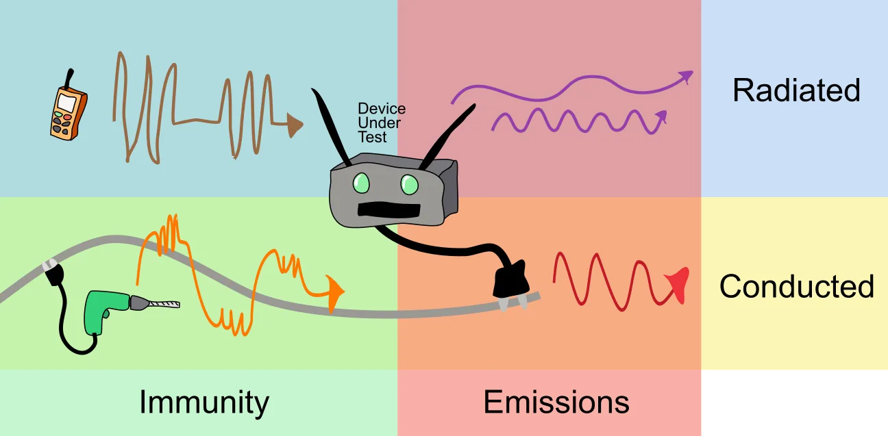
EMI refers to electromagnetic energy that disrupts the operation of electronic devices. It can manifest as radiated EMI, which propagates through the air as electromagnetic waves, or conducted EMI, which travels through power lines, cables, or PCB traces. Common sources of EMI in PCBs include high-speed digital signals, switching power supplies, and clock circuits. For instance, a signal switching at 1 GHz can generate harmonics that radiate noise, potentially interfering with nearby devices.
What is EMC?
EMC is the ability of a PCB to function correctly in its intended electromagnetic environment without causing or suffering from unacceptable interference. EMC encompasses two aspects: emission (controlling the EMI generated by the PCB) and immunity (ensuring the PCB can withstand external EMI). Regulatory standards, such as CISPR 22 for information technology equipment or IEC 61000 for industrial devices, set limits on both radiated and conducted emissions and define immunity requirements.
Why EMI/EMC Testing is Critical
EMI/EMC testing verifies that a PCB meets regulatory standards and performs reliably in its operational environment. Failing to comply can result in severe consequences:
-
Regulatory Penalties: Non-compliant products may face fines, recalls, or bans from markets like the EU or US.
-
Performance Issues: EMI can degrade signal integrity, causing data errors or system failures. For example, crosstalk in a high-speed USB 3.0 interface (5 Gbps) can lead to bit errors if not mitigated.
-
Costly Redesigns: EMC testing can cost $10,000–$50,000 per evaluation. Failing tests often requires layout changes, additional prototyping, and retesting, delaying time-to-market.
By integrating EMI/EMC considerations into the design phase, engineers can minimize these risks. Pre-compliance testing, using tools like spectrum analyzers or near-field probes, can identify issues early, reducing the likelihood of expensive failures during formal certification.
Key Sources of EMI in PCB Designs
Understanding the sources of EMI is the first step toward effective mitigation. Here are the primary culprits in PCB designs:
-
High-Speed Signals: Traces carrying signals above 50 MHz, such as DDR memory lines, can act as antennas, radiating EMI.
-
Switching Circuits: Pulse-width modulation (PWM) circuits or DC-DC converters generate high-frequency noise due to rapid switching (e.g., 500 kHz–2 MHz).
-
Ground Loops: Inconsistent grounding creates loops that radiate magnetic fields, inducing noise in nearby circuits.
-
Cables and Connectors: Long cables can act as antennas, emitting or receiving EMI. For example, an unshielded USB cable can radiate noise at 480 MHz for USB 2.0.
-
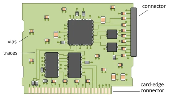
Poor PCB Layout: Large loop areas, inadequate trace spacing, or split ground planes can amplify EMI.
PCB Design Strategies for EMI/EMC Compliance
To achieve EMC compliance, engineers must adopt design practices that minimize EMI. Below are proven strategies, supported by specific techniques and examples.
1. Optimize PCB Stackup
A well-designed stackup is the foundation of low-EMI PCB design. For a 4-layer PCB, a common configuration is:
-
Top Layer: Signal traces
-
Layer 2: Ground plane
-
Layer 3: Power plane
-
Bottom Layer: Signal traces
This setup ensures that high-speed signals are adjacent to a continuous ground plane, providing a low-impedance return path. For example, a 1.6 mm FR4 PCB with a 4-layer stackup can reduce radiated emissions by 10–20 dB compared to a 2-layer board due to better signal confinement. Avoid splitting ground planes, as gaps can create high-impedance paths, increasing EMI.
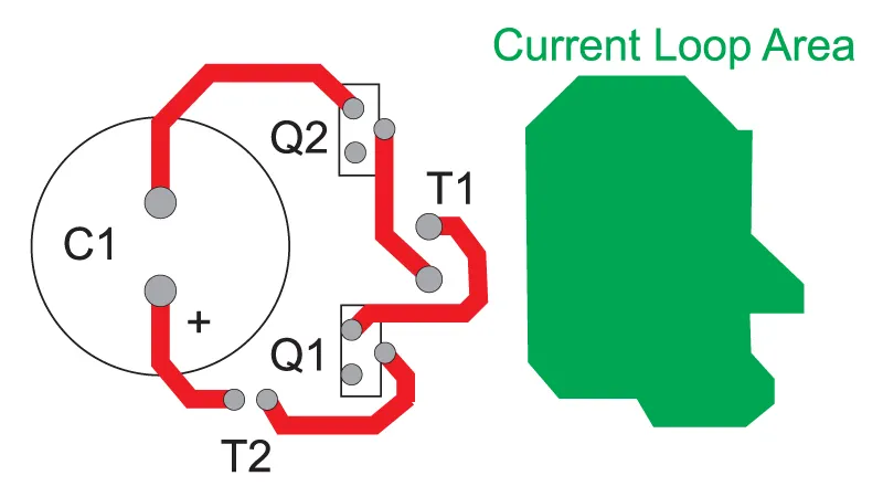
2. Minimize Loop Areas
Current loops are a major source of radiated EMI. To reduce loop areas:
-
Place decoupling capacitors (e.g., 0.1 µF ceramic) as close as possible to IC power pins, ideally within 2 mm, to minimize power loop inductance.
-
Keep signal traces short and route them over continuous ground planes. For instance, a 10 cm trace carrying a 100 MHz signal can radiate significantly if not properly referenced to ground.
-
Use via stitching to connect ground planes, reducing loop inductance. A spacing of λ/20 (where λ is the wavelength of the highest signal frequency) is effective.
3. Implement Proper Grounding
A solid ground plane is critical for EMI control. Best practices include:
-
Use a continuous ground plane on one layer to provide a low-impedance return path.
-
Avoid routing traces over splits in the ground plane, as this can cause return currents to take longer paths, increasing EMI.
-
Separate analog and digital grounds to prevent noise coupling. Connect them at a single point, typically near the power supply, to minimize ground loops.
For example, in a mixed-signal PCB, isolating the analog ground for a 16-bit ADC can reduce noise by up to 30 dB, improving signal-to-noise ratio.
Suggested Reading: The Ultimate Guide to PCB Ground Planes: Boost Signal Integrity and Reduce EMI
4. Control Signal Integrity
High-speed signals are prone to EMI due to their fast rise times (e.g., 1 ns for a 1 GHz signal). To mitigate:
-
Use controlled impedance traces (e.g., 50 Ω for single-ended or 100 Ω for differential pairs) to prevent reflections.
-
Route high-speed signals (e.g., PCIe at 8 Gbps) between ground planes to minimize crosstalk and radiation.
-
Add termination resistors (e.g., 50 Ω) to match trace impedance, reducing signal reflections that can radiate EMI.
5. Apply Shielding and Filtering
Shielding and filtering are effective for reducing EMI:
-
Shielding: Use metal enclosures or copper shields over noisy components, such as switching regulators. A shield connected to ground can attenuate radiated EMI by 20–40 dB.
-
Filtering: Place EMI filters (e.g., ferrite beads or LC filters) on power lines and I/O interfaces. For example, a ferrite bead with 600 Ω impedance at 100 MHz can suppress conducted EMI from a power supply.
-
Cable Management: Use shielded cables and ensure connectors are grounded. A 360° shield connection can reduce cable emissions by 15 dB.
Suggested Reading: EMI/EMC Shielding Strategies for Automotive PCBs: Protecting Critical Electronic Systems
6. Leverage Simulation Tools
EMI/EMC simulation tools, such as Ansys SIwave or Cadence Sigrity, allow engineers to predict and mitigate EMI before prototyping. These tools analyze:
-
Signal integrity for high-speed traces.
-
Power distribution network (PDN) noise.
-
Radiated emissions from traces and components.
For instance, simulating a 4-layer PCB with a 1 GHz clock signal can identify potential EMI hotspots, enabling layout adjustments before fabrication. Pre-compliance testing with near-field probes can further validate the design, catching issues that simulations might miss.
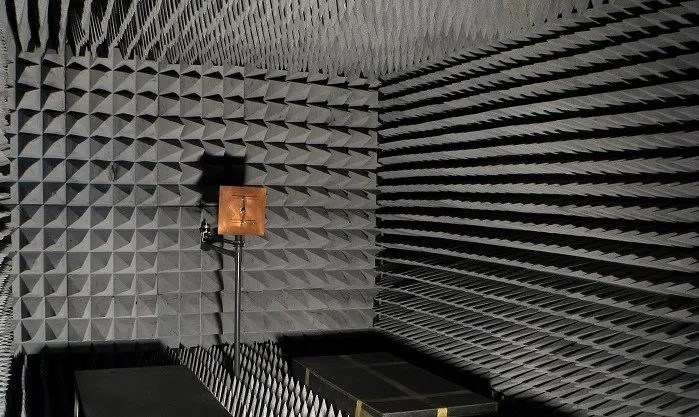
The EMI/EMC Testing Process
EMI/EMC testing is typically conducted in accredited laboratories using specialized equipment, such as anechoic chambers, spectrum analyzers, and ESD guns. The process includes:
-
Radiated Emissions Testing: Measures electromagnetic waves emitted by the PCB (30 MHz–6 GHz) against standards like CISPR 32. Limits are typically 40 dBµV/m at 3 meters for residential environments.
-
Conducted Emissions Testing: Evaluates noise conducted through power lines (150 kHz–30 MHz) per CISPR 11. Limits are around 66 dBµV for industrial devices.
-
Radiated Immunity Testing: Exposes the PCB to external electromagnetic fields (80 MHz–6 GHz) to ensure it operates correctly, per IEC 61000-4-3.
-
Conducted Immunity Testing: Tests the PCB’s resilience to conducted noise on power and signal lines.
-
ESD Testing: Simulates electrostatic discharges (e.g., 8 kV contact discharge) to verify robustness, per IEC 61000-4-2.
Pre-compliance testing in-house can reduce the risk of failure. For example, using a spectrum analyzer to measure emissions from a prototype can identify frequencies (e.g., 120 MHz harmonics) that exceed limits, allowing corrective action before formal testing.
Common Challenges and Solutions
Despite best efforts, EMI/EMC issues can arise. Here are common challenges and how to address them:
-
Late Detection of EMI: If EMI is identified during testing, review the PCB layout for large loops or poor grounding. Adding ferrite beads or shielding can help, but layout changes are often needed.
-
Unexpected Test Failures: Failures at specific frequencies (e.g., 200 MHz) may point to clock harmonics or switching noise. Use a near-field probe to locate the source and apply filters or reroute traces.
-
Costly Iterations: Multiple test cycles can be avoided by conducting pre-compliance testing early. Investing $2,000–$5,000 in in-house testing can save $20,000 in redesign costs.
How ALLPCB Supports EMI/EMC Compliance
At ALLPCB, we understand the challenges of achieving EMI/EMC compliance in PCB designs. Our advanced manufacturing capabilities, quick-turn prototyping, and global logistics empower engineers to iterate designs rapidly and meet stringent regulatory requirements. Whether you need high-quality 4-layer PCBs with precise impedance control or fast prototyping to validate EMI mitigation strategies, ALLPCB delivers reliable solutions. Our online platform streamlines the process, offering instant quotes and DFM (Design for Manufacturability) feedback to ensure your PCB layout aligns with EMC best practices, helping you get to market faster.
Conclusion
EMI/EMC testing is a critical step in ensuring that PCB designs meet regulatory standards and perform reliably in complex electromagnetic environments. By understanding EMI sources, adopting best design practices—like optimized stackups, proper grounding, and effective shielding—and leveraging simulation and pre-compliance testing, engineers can minimize risks and achieve compliance efficiently. At ALLPCB, we're committed to supporting engineers with the tools and services needed to create robust, compliant PCBs. Start your next project with confidence, knowing that EMI/EMC considerations are within reach.


