 ALLPCB


Radio Frequency (RF) Printed Circuit Boards (PCBs) are the backbone of modern wireless communication systems, powering everything from 5G networks to radar and IoT devices. Unlike standard PCBs, RF PCBs operate at high frequencies—typically 300 kHz to 300 GHz—where signal integrity, noise sensitivity, and impedance control become critical. Designing these boards is often described as a 'black art' due to the unique challenges posed by high-frequency signals. In this blog, we explore the key obstacles in RF PCB design and provide practical solutions to help engineers achieve reliable, high-performance boards.
Understanding RF PCB Design Challenges
RF PCBs differ significantly from conventional PCBs because high-frequency signals are highly sensitive to noise, impedance mismatches, and electromagnetic interference EMI compliance testing. These boards often integrate analog and digital components, creating mixed-signal environments that amplify design complexity. Below, we outline the primary challenges engineers face when designing RF PCBs.
Signal Integrity Issues
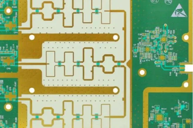
High-frequency signals are prone to degradation due to impedance mismatches, reflections, and crosstalk. For example, a mismatch between a 50-ohm trace and an RF component can cause signal reflections, leading to power loss and reduced performance. Crosstalk, where signals from adjacent traces couple unintentionally, can introduce noise and corrupt data, especially in dense layouts operating above 1 GHz.
Material Selection
Standard FR-4 materials, with a dielectric constant (Dk) of around 4.4 and a high loss tangent (0.02), are unsuitable for high-frequency applications due to significant signal loss. At frequencies above 1 GHz, FR-4's dielectric properties vary, causing impedance fluctuations. Selecting the right substrate—like Rogers RO3000 (Dk ~3.0, loss tangent ~0.001)—is crucial for minimizing losses and ensuring stable performance.
Thermal Management
RF components, such as power amplifiers, generate substantial heat, which can alter the dielectric properties of the PCB material and degrade performance. For instance, a temperature increase of 50°C can shift the Dk of some materials by up to 5%, affecting signal propagation. Inadequate thermal management can also lead to component failure in high-power applications.
EMI and Noise Sensitivity
High-frequency signals are susceptible to EMI from nearby traces, components, or external sources. For example, an improperly grounded RF trace can act as an antenna, picking up unwanted signals. Mixed-signal designs, where digital clocks operate at 1 MHz or higher, can introduce noise that disrupts sensitive analog RF circuits.
Manufacturing Tolerances
RF PCBs require tight impedance tolerances, often within ±10% of the target value (e.g., 50 ohms). Variations in trace width, dielectric thickness, or layer alignment during fabrication can lead to impedance mismatches. For instance, a 0.1 mm deviation in trace width can alter impedance by 5 ohms, significantly impacting performance at 10 GHz.
Solutions for RF PCB Design Challenges
To overcome these challenges, engineers must adopt specialized design techniques, select appropriate materials, and leverage advanced tools. Below, we provide actionable solutions tailored to each challenge.
Ensuring Signal Integrity
- Controlled Impedance Design: Calculate trace widths and dielectric thicknesses to match the target impedance (typically 50 or 75 ohms). For a 50-ohm microstrip on a Rogers RO4003C substrate (Dk = 3.38, thickness = 0.508 mm), a trace width of approximately 0.9 mm is required. Use PCB design software like Cadence Allegro or Altium Designer to verify impedance.
- Minimize Trace Lengths: Keep RF traces as short as possible to reduce signal attenuation. For example, at 10 GHz, a 10 mm trace on RO3000 can introduce 0.1 dB of loss. Use curved bends (45-degree or chamfered) instead of sharp 90-degree turns to avoid reflections.
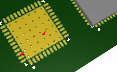
- Via Optimization: Limit the number of vias, as each via introduces ~0.5 pF of capacitance. For layer transitions, use multiple vias (e.g., two or three) to reduce inductance by up to 50%. Ensure via diameters are between 8–16 mils to minimize parasitic effects.
Suggested Reading:Signal Integrity Issues and Solutions in High-Speed PCB Design
Selecting High-Performance Materials
- Low-Loss Substrates: Choose materials like Rogers RO3000, RO4000, or PTFE-based laminates for frequencies above 1 GHz. These materials offer low loss tangents (0.001–0.003) and stable Dk values, reducing signal loss by up to 50% compared to FR-4.
- Ceramic Substrates: For high-power applications, use ceramic substrates like alumina, which provide excellent thermal conductivity (20–30 W/mK) and stable dielectric properties under thermal stress.
- Hybrid Stack-Ups: Combine materials in multilayer designs to balance cost and performance. For example, use Rogers laminates for RF layers and FR-4 for digital layers, ensuring proper isolation between analog and digital sections.
Suggested Reading:The Ultimate Guide to RF PCB Material Selection: Dk, Df, and More
Effective Thermal Management
- Thermal Vias and Planes: Incorporate thermal vias filled with copper or epoxy under high-power components to transfer heat to a solid copper plane. For a power amplifier dissipating 5 W, a grid of 10 thermal vias (0.3 mm diameter) can reduce temperature by 20°C.
- Heat Sinks and Spreaders: Use aluminum or copper heat sinks to increase surface area for heat dissipation. For critical applications, integrate chemical vapor deposition (CVD) diamond heat spreaders, which offer thermal conductivity up to 2000 W/mK.
- Wide Bandgap Materials: Employ gallium nitride (GaN) or silicon carbide (SiC) components, which operate efficiently at high temperatures with minimal power loss, reducing thermal stress on the PCB.
Mitigating EMI and Noise
- Dedicated Ground Planes: Place a continuous ground plane directly beneath RF traces to provide a low-inductance return path. For example, a 10 mm trace without a ground plane can exhibit 27 ohms of inductive reactance at 1 GHz.
- Isolation Techniques: Physically separate RF and digital components to prevent crosstalk. Use shielding cans or grounded guard traces to isolate sensitive RF circuits. For mixed-signal designs, isolate analog and digital grounds with a single-point connection to avoid ground loops.
- Decoupling Capacitors: Place decoupling capacitors (e.g., 10 µF and 100 nF) near power pins in a star configuration to filter noise. Ensure the self-resonance frequency (SRF) of capacitors exceeds the operating frequency to avoid inductive behavior.
Precision Manufacturing
- Tight Tolerances: Work with manufacturers who can maintain trace width tolerances within ±0.025 mm and dielectric thickness within ±0.05 mm to ensure consistent impedance.
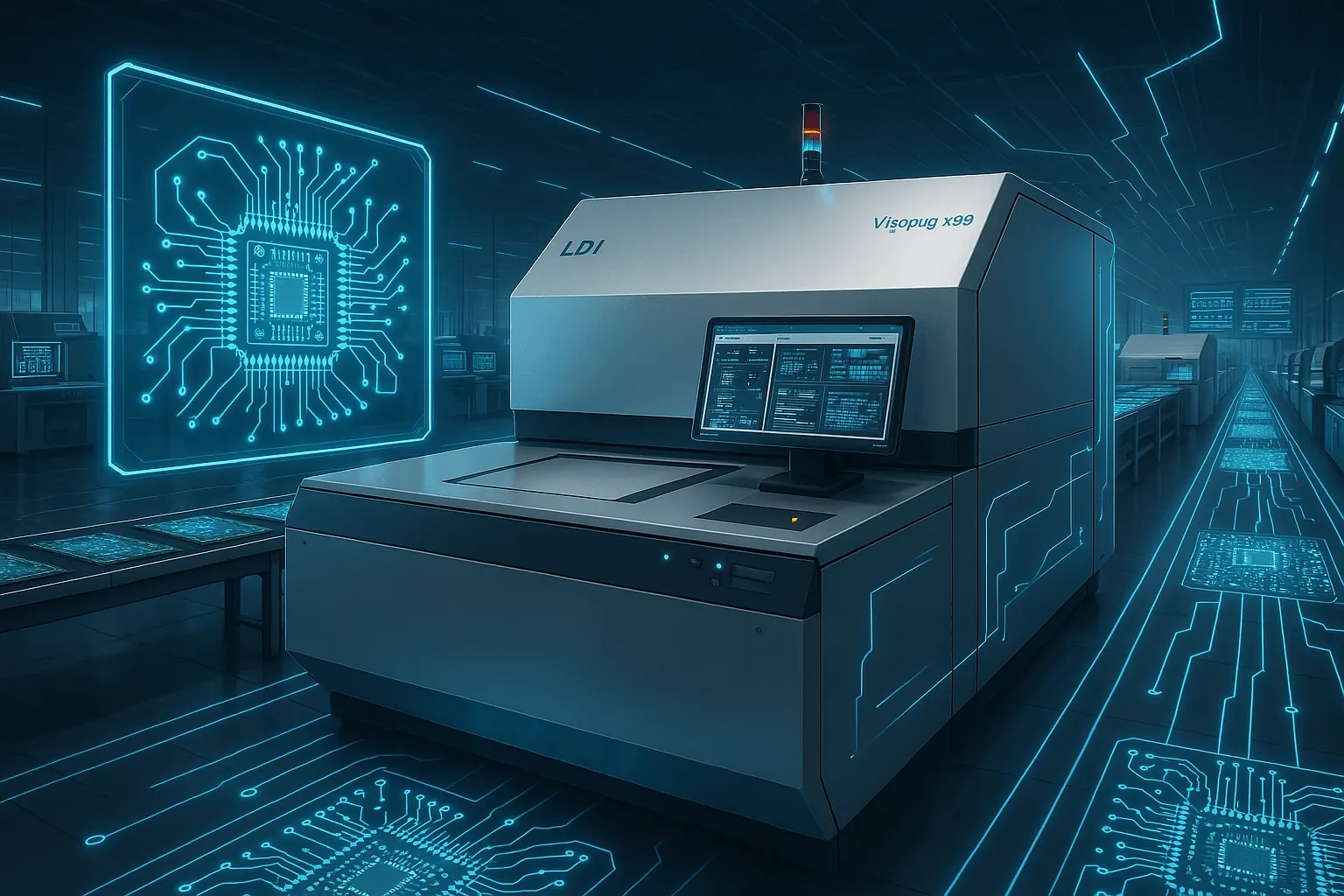
- Advanced Fabrication: Use laser direct imaging (LDI) and plasma etching for precise trace patterns and layer alignment. For frequencies above 90 GHz, employ advanced techniques like via fences to minimize coupling.
- Quality Control: Perform high-frequency measurements, such as time-domain reflectometry (TDR), to verify impedance and signal integrity before assembly.
Best Practices for RF PCB Design
To streamline the design process and enhance performance, engineers should follow these best practices:
- Start with Stack-Up Design: Define the layer stack-up early, ensuring RF traces are on the top layer, followed by a ground plane, power plane, and non-RF traces on the bottom. A 6–12 layer stack-up is typical for RF PCBs.
- Use Simulation Tools: Leverage tools like Ansys HFSS or Cadence Microwave Office for electromagnetic (EM) and signal integrity analysis. Simulate impedance, crosstalk, and EMI to identify issues before fabrication.
- Component Placement: Place RF components first, orienting them to minimize trace lengths. Keep high-power and low-power circuits separated, and position RF input and output components far apart to avoid spurious signals.
- Regulatory Compliance: Design with FCC and UL standards in mind, incorporating robust guard bands for emissions and susceptibility. Engage RF engineers early to address compliance issues.
How ALLPCB Supports RF PCB Design
For engineers tackling the complexities of RF PCB design, partnering with a reliable manufacturer is essential. At ALLPCB, we specialize in high-frequency PCB fabrication, offering quick-turn prototyping to accelerate your design cycle. Our advanced manufacturing capabilities, including precise impedance control and plasma etching, ensure your RF PCBs meet stringent performance requirements. With global logistics and a commitment to quality, we deliver tailored solutions that help engineers bring high-performance RF designs to market efficiently.
Future Trends in RF PCB Design
The demand for RF PCBs is growing with the rise of 5G, IoT, and autonomous systems. Emerging trends include:
- Flexible and Wearable PCBs: Enabling compact, lightweight RF designs for medical and consumer applications.
- Integrated Active/Passive Components: Embedding components within the PCB to reduce size and improve performance.
- Advanced Materials: Developing substrates with even lower loss tangents and higher thermal conductivity for next-generation applications.
Conclusion
RF PCB design is a complex but rewarding endeavor that requires careful attention to signal integrity, material selection, thermal management, and EMI mitigation. By adopting the solutions and best practices outlined above, engineers can overcome the challenges of high-frequency applications and deliver reliable, high-performance boards. As wireless technologies continue to evolve, staying ahead of design trends and leveraging advanced tools and manufacturing capabilities will be key to success. At ALLPCB, we're here to support your RF PCB journey with expertise and precision.


