 ALLPCB


Introduction
As electronic devices shrink in size and grow in power, managing heat dissipation in printed circuit boards (PCBs) has become a critical challenge for engineers. High-power components like processors, LEDs, and power regulators generate significant heat, and without proper thermal management, this can lead to performance degradation, shortened component lifespans, or outright failure. One of the most effective solutions we rely on in PCB design is the use of thermal vias—small, conductive pathways that transfer heat away from hot spots to cooler areas of the board. In this blog, we'll dive into the science behind thermal vias, their design considerations, and practical tips for optimizing heat dissipation in high-power PCBs.
For engineers working on cutting-edge applications—whether it's aerospace systems, automotive electronics, or high-performance computing—understanding how to implement thermal vias can make the difference between a reliable product and a costly redesign. Let's explore how these tiny features pack a big punch in thermal management.
1. What Are Thermal Vias and Why They Matter?
1.1 What Are Thermal Vias?
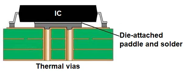
A thermal via is a plated through-hole (PTH) designed primarily for thermal conductivity rather than electrical signal transmission. Typically filled or lined with copper—whose thermal conductivity (~385 W/m·K) is vastly higher than standard FR4 substrate (~0.3 W/m·K)—these vias act like miniature heat pipes.
Their core function is to conduct heat away from a high-power component's thermal pad and transfer it to a larger copper plane, heat sink, or even the opposite side of the board where convection and radiation can dissipate it into the surrounding air.
Key difference from signal vias:
-
Signal vias: Focus on electrical performance, impedance, and trace routing.
-
Thermal vias: Focus on low thermal resistance and efficient conduction.
1.2 Why Do Thermal Vias Matter?
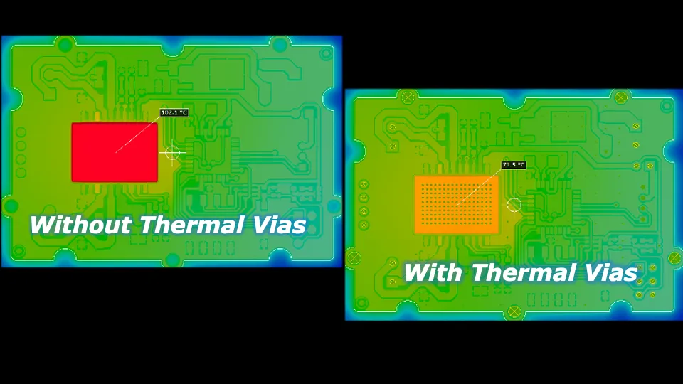
In high-power PCBs, components can reach temperatures exceeding 100°C, far above the safe operating limits of most electronics (typically 85°C for standard components). Excessive heat can reduce a component's lifespan by half for every 10°C increase beyond its rated temperature, according to the Arrhenius equation. Thermal vias help mitigate this by spreading heat across the board, preventing localized hot spots that could compromise reliability.
Read more: The Ultimate Guide to Thermal Via Placement: Cooling Your PCB Effectively
2. How Thermal Vias Work: The Science of Heat Transfer
Heat dissipation in PCBs relies on three fundamental mechanisms: conduction, convection, and radiation. Thermal vias primarily enhance conduction—the transfer of heat through a solid material. When a high-power component like a MOSFET generates heat, it flows into the copper pad beneath it. Without thermal vias, this heat would remain trapped near the surface due to the low thermal conductivity of standard PCB substrates like FR4 (around 0.3 W/m·K). Thermal vias bridge this gap by creating a vertical pathway to a larger copper plane or heat sink, where the heat can spread out and dissipate more effectively.
The effectiveness of thermal vias depends on several factors:
- Copper Plating Thickness: A thicker copper layer (e.g., 1 oz/ft² or 35 µm) improves conductivity compared to thinner layers (e.g., 0.5 oz/ft² or 17 µm).
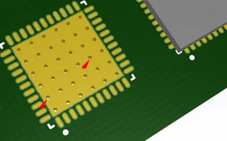
- Via Diameter: Larger vias (e.g., 0.3 mm) conduct more heat than smaller ones (e.g., 0.1 mm), though they take up more space.
- Number of Vias: An array of 6x6 vias under a component can reduce junction temperature by up to 4.8°C compared to a single via, based on thermal simulation studies.
- Placement: Positioning vias directly under the heat source maximizes efficiency.
By connecting to a ground plane or heat sink, thermal vias also enable horizontal heat spreading, leveraging the copper's large surface area to enhance convection and radiation into the surrounding air.
For SMT applications like QFN or DFN packages, see our detailed step-by-step design guide: Optimizing Thermal Vias for SMT Components: A Step-by-Step Guide
3. Designing Thermal Vias for Optimal Performance
Incorporating thermal vias into a high-power PCB isn't as simple as drilling a few holes. Engineers must balance thermal performance with electrical integrity, manufacturing constraints, and cost. Here are key design considerations:
3.1 Via Size and Spacing
Smaller vias (0.1–0.3 mm in diameter) allow for higher density, fitting more pathways under a component. However, larger vias transfer heat more effectively due to their greater cross-sectional area. A common approach is to use an array of smaller vias—say, 16 vias in a 4x4 grid—spaced 1 mm apart. This balances heat transfer with board real estate. Too close, and you risk structural weakening; too far, and heat transfer suffers.
3.2 Via Filling Options
Unfilled vias are cost-effective but can wick solder during assembly, reducing thermal contact. Filled vias, capped with copper or plugged with conductive epoxy, prevent this issue and improve heat conduction. For boards thicker than 0.7 mm, filled vias placed directly under a thermal pad can reduce thermal resistance by up to 20%.
3.3 Connection to Copper Planes
Thermal vias work best when tied to a large copper plane, such as a ground layer. This plane acts as a heat spreader, distributing energy across a wider area. Avoid thermal relief patterns (spokes) around vias unless soldering ease is a priority, as they increase thermal resistance by limiting copper contact.
3.4 Placement Strategy
Position thermal vias directly beneath or near the heat source, such as the thermal pad of a QFN package. For larger components, additional vias around the periphery can enhance dissipation. Simulations show that a 6x6 via array under a 2.5W device can lower junction temperature by 4.8°C, while a 4x4 array increases it by 2.2°C—small differences that matter in high-power designs.
Case Study: Case Studies: Successful PCB Cooling Strategies Using Thermal Vias
4. Troubleshooting Thermal Vias
Even well-designed vias may need adjustments. Key steps:
-
Identify Hot Spots: Thermal imaging or IR sensors.
-
Analyze Via Effectiveness: Check density and copper connectivity.
-
Inspect Manufacturing Quality: Plating, filling, soldering defects.
-
Reevaluate Layout: Ensure sufficient coverage.
-
Simulate Thermal Flow: Use Cadence or Altium tools.
Detailed guide: Thermal Via Troubleshooting: Diagnosing and Fixing PCB Hotspots
5. Applications of Thermal Vias in Different Industries
5.1 High-Brightness LEDs
High-power LEDs convert over 60% of electrical energy into heat. Without proper thermal management, this can reduce brightness and shorten lifespan. Thermal vias efficiently transfer heat from the LED pad to copper planes or metal cores, maintaining performance and longevity.
Read more here: Thermal Vias in LED Lighting PCBs: Keeping Your LEDs Cool and Efficient
5.2 Retail Technology
Devices in retail environments, such as POS terminals, scanners, and digital signage, often operate continuously and generate substantial heat. Proper via placement ensures consistent operation and prevents thermal throttling in sensitive electronics.
Read more here: Thermal Vias for Cooling Retail Tech: A PCB Design Guide.
5.3 Aerospace & Automotive
Extreme environments demand robust thermal management—filled VIPPO vias and metal-core PCBs are often used.
6. Benefits of Thermal Vias in High-Power PCBs
Thermal vias offer several advantages that make them indispensable in high-power applications:
- Improved Reliability: By keeping temperatures below critical thresholds (e.g., 85°C), they extend component life.
- Cost-Effective Cooling: Unlike external heat sinks or fans, thermal vias add no extra parts, reducing assembly complexity.
- Space Efficiency: They fit within the PCB footprint, ideal for compact designs like wearables or IoT devices.
- Enhanced Performance: Lower temperatures prevent thermal throttling in processors and LEDs, maintaining peak efficiency.
7. Challenges and Limitations
While thermal vias are powerful tools, they're not without trade-offs:
- Manufacturing Complexity: Filled or capped vias increase the custom PCB board cost and require precise processes to avoid defects.
- Electrical Interference: Connecting vias to a ground plane can introduce capacitance, affecting high-frequency signals.
- Limited Heat Capacity: In extreme cases (e.g., >10W components), thermal vias alone may not suffice, necessitating additional cooling like heat sinks or forced air.
Engineers must weigh these factors against the application's needs. For instance, a high-frequency RF board might prioritize signal integrity over dense via arrays, while a power supply PCB might maximize via count.
8. Practical Tips for Implementing Thermal Vias
Ready to add thermal vias to your next high-power PCB? Here are actionable steps to get started:
1. Analyze Heat Sources: Use manufacturer datasheets to identify components with high power dissipation (e.g., >1W) and their thermal pad requirements.
2. Simulate Early: Tools like Cadence or Altium's thermal solvers can model heat flow, showing how расход via count and placement affect temperature. Aim for a junction temperature at least 20°C below the maximum rating.
3. Follow Guidelines: For QFN or DFN packages, adhere to datasheet recommendations—typically 9–25 vias in a grid pattern.
4. Optimize Copper: Pair vias with thick copper layers (e.g., 2 oz/ft²) for better heat spreading.
5. Test Prototypes: Use thermal imaging cameras to verify performance and spot hot spots on physical boards.
DIY Guide: DIY Thermal Vias: A Simple Guide for Hobbyist PCB Projects
9. Advanced Techniques: Beyond Basic Thermal Vias
For extreme heat challenges, engineers can push thermal vias further:
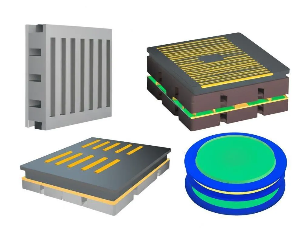
- Microvias: Stacked or staggered microvias in HDI (high-density interconnect) boards increase via density in tight spaces.
- Metal Core PCBs (MCPCBs): Pairing thermal vias with an aluminum or copper core (thermal conductivity ~200 W/m·K) boosts dissipation for applications like high-power LEDs.
- Via-in-Pad: Placing filled vias directly under a component's pad minimizes thermal resistance, ideal for boards over 1.6 mm thick.
These techniques shine in aerospace or automotive designs, where reliability under harsh conditions is non-negotiable.
Emerging Trends: The Future of Thermal Vias: Emerging Technologies in PCB Cooling
10. How ALLPCB Supports Thermal Management in PCB Design
For engineers tackling high-power PCB projects, partnering with a reliable manufacturer can streamline the process. At ALLPCB, we offer advanced manufacturing capabilities like precision via drilling and copper plating to ensure your thermal vias perform as designed. Our quick-turn prototyping lets you test thermal management strategies fast, while our global logistics ensure timely delivery—critical when iterating on heat-sensitive designs. Whether you're building a compact IoT device or a robust power supply, our expertise helps bring your thermal via concepts to life with precision and efficiency.
Conclusion
Thermal vias are a cornerstone of effective high-power PCB thermal management, offering a simple yet powerful way to keep temperatures in check. By understanding their mechanics, designing them thoughtfully, and pairing them with the right materials and tools, engineers can create reliable, high-performing electronics. From via size and placement to advanced techniques like MCPCBs, every detail counts in the fight against heat.
As power densities rise and designs grow more complex, thermal vias will remain a go-to solution. Start integrating them into your next project, simulate their impact, and see the difference they make. Have questions or need help optimizing your PCB's thermal performance? We're here to assist—reach out and let's tackle the heat together.


