 ALLPCB


Printed circuit boards (PCBs) are the backbone of modern electronics, and every detail in their design can impact performance, reliability, and manufacturability. One such detail is edge plating, a specialized technique that involves applying a metallic coating, typically copper, along the edges of a PCB. This process enhances electrical connectivity, improves electromagnetic compatibility (EMC), and supports unique mechanical requirements. In this blog, we explore the applications of edge plating, provide actionable design guidelines, and share insights to help engineers optimize their PCB designs.
Whether you're designing high-frequency RF boards, compact IoT devices, or robust industrial systems, understanding edge plating can elevate your project's performance. Let's dive into what makes this technique essential and how to implement it effectively.
What is PCB Edge Plating?
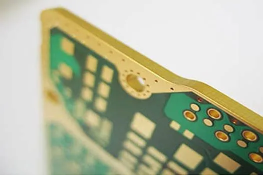
Edge plating, also known as side plating, castellation, or metallized edge plating, involves electroplating a conductive material—typically copper—along the perimeter edges of a PCB, connecting the top and bottom surfaces. This creates a continuous conductive path that can extend along one or more edges, or even wrap around internal cutouts. Unlike standard through-hole plating, edge plating focuses on the board's exterior or specific slots, serving both electrical and mechanical purposes.
The process begins with routing the PCB profile where plating is needed, followed by electroplating during the through-hole plating stage. A surface finish, such as Electroless Nickel Immersion Gold (ENIG), is often applied to enhance durability and solderability. Edge plating is common in applications requiring EMI shielding, robust grounding, or board-to-board connections, but it demands precision to avoid issues like burrs or peeling.
Key Applications of Edge Plating in PCBs
Edge plating serves multiple purposes, making it a versatile solution for various industries. Below, we outline its primary applications, supported by practical examples.
1. Electromagnetic Interference (EMI) Shielding
In high-frequency designs, such as RF PCBs operating in the megahertz to gigahertz range, EMI can degrade signal integrity. Edge plating creates a conductive shield along the board's perimeter, acting as a partial Faraday cage to contain electromagnetic fields. This is critical for applications like wireless communication devices, where signal interference can disrupt performance.
For example, in a 5G antenna module, edge plating reduces EMI by providing a continuous ground path, ensuring signals remain clean even at frequencies above 3 GHz. Without edge plating, radiation from power planes could escape, increasing noise and failing EMC compliance tests.
2. Enhanced Grounding for Signal Integrity
High-speed digital circuits, such as those using low-voltage differential signaling (LVDS) at speeds exceeding 1 Gbps, require a stable ground reference. Edge plating connects ground planes across layers, minimizing ground loops and improving signal integrity. This is especially useful in multilayer PCBs with power planes extending close to the board edge.
Consider a server motherboard with DDR5 memory running at 4800 MHz. Edge plating ensures a low-impedance ground path, reducing voltage noise and supporting reliable data transmission.
3. Board-to-Board and Edge Connections
Edge plating enables direct board-to-board connections or integration with metal enclosures. For instance, in modular electronics, edge-plated PCBs can slide into metal casings, using the plated edge as a connector. This eliminates the need for additional components, saving space and cost.
An example is a USB dongle, where gold-plated edge fingers (a form of edge plating) withstand over 5,000 insertion cycles, ensuring durability and reliable contact with the host device.
4. Thermal Management
High-power applications, such as LED lighting or power supplies, generate significant heat. Edge plating, when connected to ground planes via thermal vias, provides a large conductive surface for heat dissipation. This improves thermal performance without requiring additional cooling components.
In an automotive power module, edge plating can reduce the temperature of a 100 W circuit by up to 10°C, extending component lifespan.
Recommended Reading: Thermal Management in PCB Design: Meeting Standards for Heat Dissipation
5. Mechanical Strength and Protection
Edge plating reinforces the PCB's perimeter, protecting vulnerable edges from mechanical stress or environmental factors like moisture. This is valuable in rugged applications, such as aerospace or industrial sensors, where boards face frequent handling or harsh conditions.
For example, in a drone's flight controller, edge plating prevents edge delamination during vibrations, ensuring long-term reliability.
Design Guidelines for Effective Edge Plating
Implementing edge plating requires careful planning to ensure manufacturability and performance. Below are detailed design guidelines to help engineers avoid common pitfalls and achieve optimal results.
1. Define Plated Areas Clearly
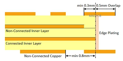
To ensure manufacturability, use overlapping copper (pads, traces, or surfaces) to define the areas to be plated. A minimum overlap of 0.5 mm (20 mils) is recommended to provide sufficient contact for the plating process. For connected layers, maintain at least 0.3 mm (12 mils) of copper overlap, and for non-connected layers, keep a gap of at least 0.8 mm (32 mils) from the board's outer contour to prevent unintended connections.
In your CAD layout, indicate edge plating requirements on a mechanical layer, specifying which edges or slots need plating. For selective plating, provide an annotated diagram in your Gerber files or fabrication drawings.
2. Maintain Clearances to Avoid Shorts
Edge plating typically connects to the ground net, but improper design can cause shorts with other nets. Maintain a minimum clearance of 0.25 mm (10 mils) between the plated edge and any different-net copper features, such as signal traces or power planes. For power planes, pull back the plane by at least 0.2 mm (8 mils) from the board edge to avoid contact with the plating.
For edge-mounted connectors, like SMA connectors, use a polygon cutout around the pad to prevent the plating from extending over it, which could cause a short circuit.
3. Remove Solder Mask Along Plated Edges
To ensure proper plating and contact with external components (e.g., shielded enclosures), remove the solder mask along the plated edge. A typical solder mask pullback of 0.5–1.25 mm (20–50 mils) exposes the copper for plating and ensures reliable electrical connections. Ensure consistency in solder mask openings on both top and bottom layers.
4. Account for Manufacturing Constraints
Edge plating requires routing the board profile before through-hole plating, which precludes V-cut scoring. Instead, use tab routing, leaving gaps where rout tabs hold the board in the production panel. These gaps, typically 1–2 mm wide, mean the plating won't cover the entire edge length. Confirm with your manufacturer the extent of plating coverage and tab placement.
Additionally, avoid placing vias or plated holes near the board edge, as they can interfere with the plating process or weaken the edge structure. A minimum clearance of 0.25 mm (10 mils) is recommended.
5. Choose an Appropriate Surface Finish
The surface finish protects the plated edge and enhances solderability. ENIG is the most common choice due to its corrosion resistance and compatibility with round edge plating. For high-durability applications, such as edge connectors, consider a gold thickness of at least 50 µin to withstand thousands of mating cycles. HASL or ENEPIG are alternatives, but confirm their suitability with your manufacturer.
6. Mitigate Burrs and Peeling
Burrs—small metal protrusions from machining—can cause short circuits or reduce adhesion. To minimize burrs, ensure the board edge is smooth and clean before plating. Manufacturers can use chemical etching or proprietary polishing to achieve this. To prevent peeling, roughen the edge surface (e.g., via micro-etching) to improve adhesion, and use direct metallization for stronger copper bonding.
7. Consider High-Frequency and Thermal Effects
In RF or high-speed designs, edge plating affects controlled impedance traces near the board edge. Adjust trace widths or increase their distance from the edge (e.g., by 0.5 mm) to maintain impedance values, such as 50 ohms for RF signals. For thermal management, connect edge plating to internal ground planes with thermal vias spaced 1–2 mm apart to maximize heat flux.
Common Challenges and Solutions
Edge plating, while beneficial, introduces manufacturing and design challenges. Here are common issues and how to address them:
- Burr Formation: Burrs from routing or drilling can disrupt plating quality. Solution: Work with manufacturers who use advanced deburring techniques, such as chemical etching or polishing.
- Peeling of Plated Copper: Poor adhesion over large surfaces can cause peeling. Solution: Roughen the edge surface and use high-bond-strength metallization processes.
- Short Circuits: Power planes or traces too close to the edge can contact the plating. Solution: Enforce strict clearance rules and verify designs with DRC checks.
- Incomplete Plating: Misaligned routing or insufficient copper overlap can lead to gaps in plating. Solution: Provide clear fabrication drawings and confirm manufacturer capabilities.
By anticipating these challenges and following the guidelines above, engineers can ensure reliable edge plating.
How ALLPCB Supports Edge Plating Projects
For engineers tackling complex PCB designs, partnering with a reliable manufacturer is crucial. ALLPCB's advanced manufacturing capabilities and quick-turn prototyping services streamline the production of edge-plated PCBs. Our state-of-the-art facilities handle precision routing and plating processes, ensuring high-quality results with minimal burrs or adhesion issues. With global logistics and real-time support, we help you meet tight deadlines while maintaining strict quality standards. Whether you're designing RF modules or rugged industrial boards, ALLPCB's expertise empowers you to bring your vision to life.
Conclusion
Edge plating is a powerful technique that enhances PCB performance across EMI shielding, signal integrity, thermal management, and mechanical reliability. By understanding its applications and adhering to design guidelines, engineers can unlock its full potential while avoiding common pitfalls. From defining plated areas to choosing the right surface finish, every step requires attention to detail and collaboration with your manufacturer.
As electronics continue to evolve, edge plating will remain a critical tool for meeting the demands of high-speed, compact, and robust designs. We hope this guide equips you with the knowledge to implement edge plating effectively in your next project.


