 ALLPCB


Sequential build-up (SBU) PCBs are advanced multilayer boards created by adding layers one at a time, enabling high-density interconnects (HDI) and complex designs for cutting-edge electronics. Now, let’s explore this fascinating technology in detail to help you master it for your projects.
What Are Sequential Build-Up PCBs and Why Do They Matter?
Sequential build-up (SBU) PCBs are a cornerstone of modern electronics, especially for high-performance and compact devices like smartphones, medical equipment, and aerospace systems. Unlike traditional multilayer PCBs, where all layers are laminated at once, SBU technology involves adding layers sequentially, one or two at a time. This method allows for intricate via structures, finer traces, and higher circuit density, making it ideal for advanced applications.
The importance of SBU PCBs lies in their ability to support high-density interconnects (HDI). With the demand for smaller, faster, and more efficient electronics, SBU technology ensures that designers can pack more functionality into limited space. Whether it’s achieving signal speeds above 10 Gbps or managing impedance values as low as 50 ohms for high-speed designs, SBU PCBs are the go-to solution for engineers pushing the boundaries of innovation.
Understanding Sequential Build-Up PCB Design
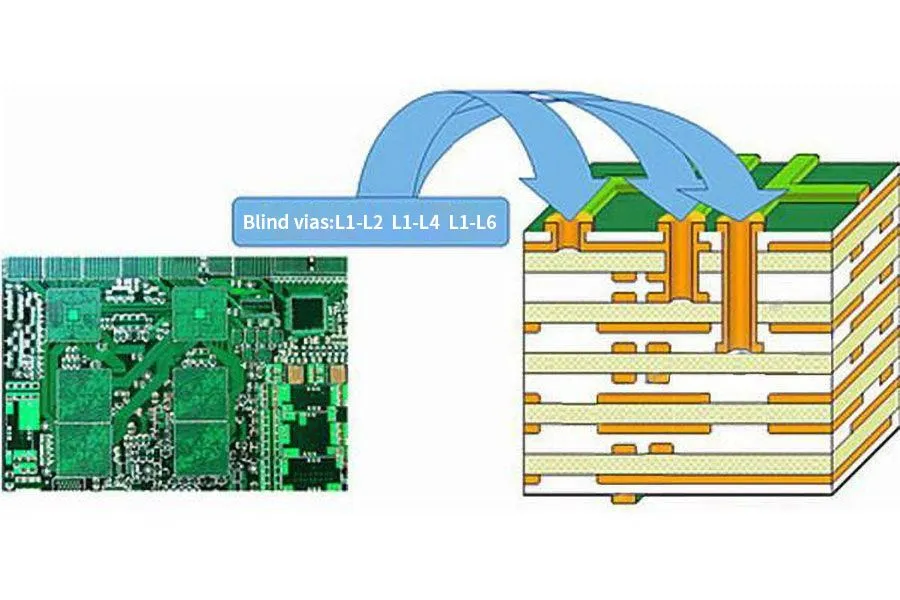
Designing a sequential build-up PCB requires precision and a deep understanding of the end application. The process starts with creating a core layer, usually a standard double-sided board, followed by the addition of insulating and conductive layers in a controlled sequence. This approach allows for the integration of microvias, blind vias, and buried vias, which are essential for connecting layers without occupying surface space.
Key considerations in sequential build-up PCB design include signal integrity, thermal management, and layer alignment. For instance, maintaining a controlled impedance of 50 ohms for high-speed signals often requires precise dielectric thickness and copper trace widths as narrow as 3 mils (0.003 inches). Designers must also account for the coefficient of thermal expansion (CTE) to prevent delamination during temperature fluctuations, especially in applications like automotive electronics where temperatures can range from -40°C to 85°C.
Software tools play a crucial role in SBU design, enabling engineers to simulate signal performance and detect potential issues before manufacturing. By optimizing the layout for minimal crosstalk and noise, designers can ensure reliable performance in advanced electronics.
The Sequential Build-Up PCB Manufacturing Process
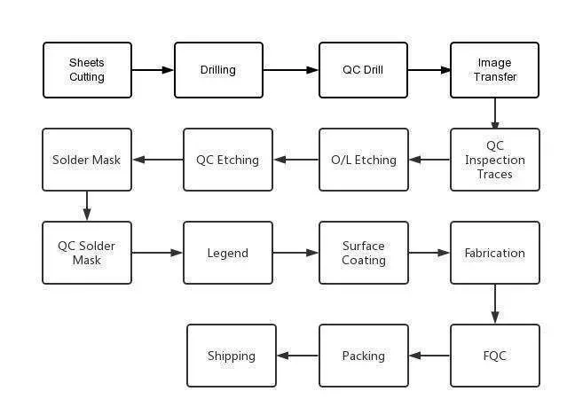
The sequential build-up PCB manufacturing process is a complex, multi-step procedure that demands precision at every stage. Here’s a detailed look at how these advanced boards come to life:
- Core Fabrication: The process begins with a core layer, typically made of a thin laminate material like FR-4 or a high-frequency alternative. This core is drilled and plated to form initial vias.
- Layer Addition: Insulating layers, often prepreg materials, are added one at a time. Each layer is laminated under heat (around 180°C) and pressure (up to 300 psi) to ensure bonding.
- Microvia Formation: Laser drilling is used to create microvias, which can be as small as 0.1 mm in diameter. These vias are then plated with copper to establish electrical connections.
- Circuit Patterning: Each layer undergoes photolithography to define copper traces. Etching removes excess copper, leaving behind fine lines with widths down to 2 mils.
- Sequential Lamination: Additional layers are added and laminated in cycles, repeating the process until the desired layer count is achieved—often 8 to 14 layers for advanced designs.
- Final Processing: The board is finished with surface treatments like ENIG (Electroless Nickel Immersion Gold) for better solderability and tested for electrical continuity.
This meticulous process ensures that SBU PCBs can handle high-frequency signals (up to 20 GHz in some cases) and meet the stringent requirements of modern electronics.
Decoding Sequential Build-Up PCB Stack-Up
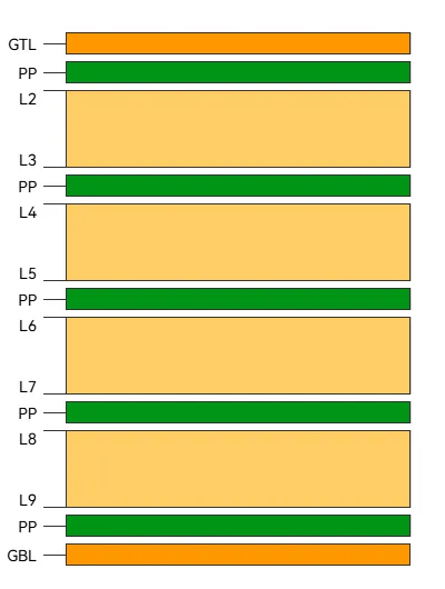
The sequential build-up PCB stack-up refers to the arrangement of conductive and insulating layers in the board. A well-planned stack-up is critical for maintaining signal integrity, minimizing electromagnetic interference (EMI), and ensuring power distribution in high-speed designs.
For example, a typical 10-layer SBU PCB stack-up might include:
- Top signal layer for component mounting.
- Ground plane to reduce noise.
- Multiple signal layers for routing high-speed traces.
- Power planes for stable voltage supply (e.g., 3.3V or 5V).
- Bottom signal layer for additional routing.
Each layer is separated by dielectric materials with specific thicknesses (often 0.1 mm to 0.2 mm) to control impedance. Microvias and blind vias connect layers without penetrating the entire board, saving space and improving routing density. Engineers often aim for symmetry in the stack-up to prevent warping during manufacturing, balancing copper distribution across layers.
In high-speed applications, such as 5G communication devices, stack-up design must account for signal propagation delays. A dielectric constant (Dk) of around 3.5 to 4.0 is common for materials used in these designs to ensure signal speeds remain consistent across frequencies.
Choosing the Right Sequential Build-Up PCB Materials
Selecting the appropriate sequential build-up PCB materials is vital for performance, reliability, and cost-effectiveness. The materials used in SBU PCBs must withstand the rigors of sequential lamination while meeting electrical and thermal requirements. Here are the key material categories:
- Core and Prepreg Materials: FR-4 is a common choice for its affordability and decent electrical properties (Dk around 4.5). For high-frequency applications, low-loss materials like polyimide or PTFE-based laminates with Dk values as low as 2.2 are preferred to minimize signal loss.
- Copper Foil: Electrodeposited (ED) copper foil with a thickness of 0.5 oz to 1 oz per square foot is typically used for conductive layers. Thinner foils reduce skin effect losses in high-frequency designs.
- Dielectric Films: Thin dielectric films are used between build-up layers to maintain controlled impedance. These films often have thicknesses of 25 to 50 micrometers.
- Surface Finishes: Finishes like ENIG or immersion silver protect copper pads and ensure reliable soldering. ENIG, for instance, offers a flat surface and excellent corrosion resistance.
Material selection also depends on the operating environment. For aerospace applications, materials with a glass transition temperature (Tg) above 170°C are chosen to handle extreme conditions. Additionally, low dissipation factor (Df) materials (below 0.005) are critical for minimizing signal attenuation in high-speed circuits.
Benefits of Sequential Build-Up PCBs in Advanced Electronics
SBU PCBs offer several advantages that make them indispensable for cutting-edge technology:
- Higher Density: With microvias and fine traces, SBU PCBs support component densities up to 100 components per square inch, perfect for compact devices.
- Improved Signal Integrity: Controlled impedance and shorter interconnects reduce signal loss, supporting data rates beyond 25 Gbps.
- Flexibility in Design: The ability to add layers sequentially allows for tailored solutions, whether it’s a 6-layer board for consumer gadgets or a 14-layer board for industrial systems.
- Reduced Size and Weight: By eliminating through-hole vias, SBU PCBs save space, contributing to lighter and smaller end products.
These benefits translate to real-world impact, enabling innovations in fields like 5G telecommunications, wearable technology, and autonomous vehicles.
Challenges in Sequential Build-Up PCB Design and Manufacturing
While SBU PCBs are powerful, they come with unique challenges:
- Complexity: The sequential lamination process increases manufacturing time and requires precise alignment to avoid defects like layer misalignment.
- Cost: Due to multiple lamination cycles and advanced materials, SBU PCBs can cost 20-30% more than standard multilayer boards.
- Thermal Stress: Repeated heating during lamination (up to 180°C) can stress materials, risking delamination if CTE values are mismatched.
- Testing: Ensuring connectivity across microvias and buried vias demands advanced testing methods like X-ray inspection.
Overcoming these challenges requires close collaboration between designers and manufacturers to optimize processes and material choices.
Tips for Successful Sequential Build-Up PCB Projects
To ensure your SBU PCB project succeeds, keep these practical tips in mind:
- Start with a detailed stack-up plan to balance signal and power layers for optimal performance.
- Use simulation tools to predict signal behavior and adjust trace widths (e.g., 4 mils for high-speed lines) and spacing accordingly.
- Choose materials based on your application’s frequency and thermal needs, such as low-Dk laminates for signals above 10 GHz.
- Work closely with your manufacturing partner to align design rules with fabrication capabilities, especially for microvia aspect ratios (typically 0.8:1).
- Test prototypes thoroughly for electrical and thermal performance before full-scale production.
By following these guidelines, you can minimize risks and achieve reliable, high-performing SBU PCBs for your advanced electronics.
Conclusion: Elevate Your Electronics with Sequential Build-Up PCBs
Sequential build-up PCBs are a game-changer for advanced electronics, offering unmatched density, signal performance, and design flexibility. By mastering sequential build-up PCB design, understanding the sequential build-up PCB manufacturing process, optimizing the sequential build-up PCB stack-up, and selecting the right sequential build-up PCB materials, you can unlock new possibilities for your projects. Whether you’re developing next-gen communication devices or compact medical equipment, SBU technology provides the foundation for innovation.
At ALLPCB, we’re committed to supporting engineers with cutting-edge solutions and expertise. Dive into the world of SBU PCBs and take your designs to the next level with precision and confidence.


