 ALLPCB


In the world of electronics, managing heat in printed circuit boards (PCBs) is crucial for ensuring performance, reliability, and longevity. Poor thermal management can lead to component failure, reduced efficiency, and even safety hazards. So, how do you design a PCB to handle heat effectively while meeting industry standards? This blog post dives deep into the essentials of thermal management in PCB design, covering key techniques like PCB thermal vias design, PCB heatsink selection, thermal simulation for PCBs, PCB material thermal conductivity, and high power PCB thermal design. Whether you're an engineer or a designer, you'll find practical tips and insights to optimize your PCB projects for heat dissipation.
Why Thermal Management Matters in PCB Design
Modern electronic devices are becoming smaller, faster, and more powerful, which means they generate more heat in confined spaces. Excessive heat can degrade components, cause thermal stress, and disrupt signal integrity. Effective thermal management ensures that your PCB operates within safe temperature limits, often defined by standards like IPC-2152 for current carrying capacity and thermal considerations. By addressing heat dissipation early in the design phase, you can prevent costly redesigns and ensure your product meets performance expectations.
Key Techniques for Effective PCB Thermal Management
Let’s explore the critical aspects of thermal management in PCB design. Each technique below is tailored to help you tackle heat dissipation challenges and align with industry best practices.
1. PCB Thermal Vias Design: Enhancing Heat Transfer
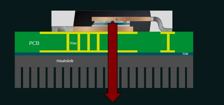
Thermal vias are small holes in a PCB filled or plated with conductive material, typically copper, to transfer heat from one layer of the board to another or to a heat sink. They act like tiny heat pipes, moving thermal energy away from hot components to cooler areas. Proper PCB thermal vias design is essential for high-power applications where components like power transistors or LEDs generate significant heat.
For optimal performance, consider the following when designing thermal vias:
- Placement: Position vias directly under or near heat-generating components to maximize heat transfer. A grid pattern often works best for uniform distribution.
- Size and Number: Use vias with a diameter of 0.3 to 0.5 mm for effective heat conduction without compromising structural integrity. The number of vias depends on the heat load—more vias for higher power components.
- Fill Material: Plated-through vias with copper are standard, but for advanced designs, filled vias (with epoxy or copper paste) can improve thermal conductivity by up to 30%.
By adhering to standards like IPC-2221, which provides guidelines for via design, you can ensure that your thermal vias effectively dissipate heat while maintaining board reliability.
2. PCB Heatsink Selection: Choosing the Right Cooling Solution
Heatsinks are passive cooling devices that absorb and dissipate heat from components through conduction and convection. PCB heatsink selection is a critical step in thermal management, especially for components with high thermal output, such as microprocessors or power amplifiers.
When selecting a heatsink, keep these factors in mind:
- Material: Aluminum is the most common heatsink material due to its high thermal conductivity (approximately 205 W/m·K) and lightweight nature. For extreme cases, copper heatsinks (thermal conductivity of 401 W/m·K) offer superior performance but at a higher cost and weight.
- Size and Shape: The heatsink size should match the component’s heat dissipation needs. Fin designs increase surface area for better cooling—pin fins work well with forced airflow, while straight fins are ideal for natural convection.
- Thermal Interface Material (TIM): Use a high-quality TIM, like thermal paste or pads, between the component and heatsink to minimize thermal resistance. A good TIM can reduce contact resistance by up to 50%.
Selecting the right heatsink also involves considering the PCB layout and available space. Ensure proper mounting to avoid mechanical stress on the board, and follow thermal design guidelines from standards like JEDEC for component-specific cooling requirements.
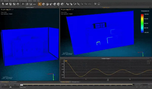
3. Thermal Simulation for PCBs: Predicting and Optimizing Performance
Thermal simulation for PCBs is a powerful tool that allows designers to predict how heat will behave in their designs before manufacturing. Using software to model heat flow, you can identify potential hot spots, test different cooling solutions, and optimize your layout for better heat dissipation.
Here’s how thermal simulation benefits PCB design:
- Hot Spot Identification: Simulations can reveal areas where temperatures exceed safe limits (often above 85°C for most components), allowing you to adjust the design early.
- Material and Layout Testing: Test different PCB materials or via arrangements to see their impact on heat distribution without building physical prototypes.
- Power Analysis: For high-power designs, simulations help ensure that current levels (e.g., 2A or higher per trace) don’t cause excessive heating, aligning with standards like IPC-2152 for trace width and temperature rise.
Most simulation tools use finite element analysis (FEA) to model heat transfer with accuracy. By inputting parameters like component power dissipation (e.g., 5W for a power IC) and ambient temperature (e.g., 25°C), you can get detailed thermal maps of your PCB. This data-driven approach saves time and reduces the risk of thermal failures in the field.
4. PCB Material Thermal Conductivity: Choosing the Right Substrate
The choice of PCB material plays a significant role in thermal management. PCB material thermal conductivity determines how effectively heat is conducted away from components. Standard FR-4 material, commonly used in PCBs, has a thermal conductivity of about 0.3 W/m·K, which is low and often insufficient for high-power applications.
For better heat dissipation, consider these alternatives:
- Metal Core PCBs (MCPCBs): These use a metal base layer, often aluminum, with a thermal conductivity of up to 2.0 W/m·K. They are ideal for LED lighting and power electronics.
- Ceramic Substrates: Materials like alumina offer thermal conductivity up to 30 W/m·K, suitable for extreme heat environments, though they are more expensive.
- High-Tg FR-4: For moderate heat applications, high-Tg variants of FR-4 provide better thermal stability (glass transition temperature above 170°C) compared to standard FR-4 (around 130°C).
Selecting a material with higher thermal conductivity reduces the temperature rise across the board. However, balance this with cost and electrical performance, as highly conductive materials can sometimes affect signal integrity. Standards like IPC-4101 provide specifications for PCB materials, ensuring compatibility with thermal and mechanical requirements.
5. High Power PCB Thermal Design: Handling Extreme Heat Loads
High power PCB thermal design is critical for applications like power supplies, motor controllers, and RF amplifiers, where components handle large currents and dissipate significant heat. Without proper design, temperatures can easily exceed safe limits, leading to failures.
Here are key strategies for managing heat in high-power PCBs:
- Thicker Copper Layers: Use thicker copper (e.g., 2 oz/ft2 or 70 μm) for power traces to reduce resistance and heat generation. According to IPC-2152, doubling copper thickness can reduce temperature rise by nearly 50% for the same current.
- Plane Layers for Heat Spreading: Dedicate internal or external layers as ground or power planes to act as heat spreaders. A solid copper plane can lower thermal resistance by up to 40% compared to a trace-only design.
- Component Spacing: Space out high-power components to prevent localized heat buildup. Maintain at least 2-3 mm clearance between heat sources to allow better airflow or heat dissipation.
- Forced Cooling: In extreme cases, integrate fans or liquid cooling systems to actively remove heat. Ensure the PCB layout accommodates mounting points for these systems without interfering with other components.
Designing for high power also means adhering to safety and performance standards. For instance, IPC-2221B provides guidelines for spacing and trace widths in high-current designs to prevent thermal runaway. By combining these techniques, you can build robust PCBs that handle high power without overheating.
Industry Standards for PCB Thermal Management
Meeting industry standards is non-negotiable when designing PCBs for thermal performance. These standards provide a framework to ensure safety, reliability, and consistency across designs. Here are some key standards to follow:
- IPC-2152: Focuses on current-carrying capacity and temperature rise in PCB traces, helping designers calculate safe trace widths for given power levels.
- IPC-2221: Offers general guidelines for PCB design, including thermal vias and component placement for heat dissipation.
- JEDEC Standards: Provide component-level thermal management guidelines, especially for semiconductors and ICs, ensuring they operate within specified temperature ranges.
By designing with these standards in mind, you not only improve the thermal performance of your PCB but also ensure compliance with industry expectations, reducing the risk of failures or recalls.
Practical Tips for Implementing Thermal Management
Beyond the core techniques, here are some additional tips to enhance your PCB thermal management strategy:
- Start thermal analysis early in the design process to identify issues before layout finalization.
- Use larger board sizes when possible to spread heat over a wider area, reducing localized hot spots.
- Consider environmental factors like ambient temperature and enclosure design, as they impact overall heat dissipation.
- Regularly update your knowledge on new materials and cooling technologies to stay ahead of thermal challenges.
Conclusion: Building Better PCBs with Thermal Management
Thermal management in PCB design is not just a technical requirement—it’s a cornerstone of creating reliable, high-performing electronics. By focusing on PCB thermal vias design, PCB heatsink selection, thermal simulation for PCBs, PCB material thermal conductivity, and high power PCB thermal design, you can tackle heat dissipation challenges head-on. Following industry standards ensures that your designs are safe and effective, while practical techniques like simulations and material choices help optimize performance.


