 ALLPCB


In today's fast-paced electronics industry, high-speed printed circuit boards (PCBs) power everything from 5G networks to AI-driven data centers. As signal speeds climb into the multi-gigabit range, ensuring signal integrity (SI) is critical to prevent data errors, system crashes, or costly redesigns. Signal integrity testing validates that signals maintain their quality across PCB traces, vias, and components, even at frequencies exceeding 10 GHz. At ALLPCB, we understand the challenges engineers face in achieving reliable high-speed PCB performance. This blog explores essential tools for signal integrity testing, offering practical insights to help you validate your designs with confidence.
What Is Signal Integrity and Why Does It Matter?
Signal integrity refers to the ability of an electrical signal to travel from transmitter to receiver without significant degradation. In high-speed PCBs, signals face challenges like crosstalk, reflections, impedance mismatches, and jitter, which can distort waveforms and cause errors. For example, a 25 Gbps signal on a PCIe 5.0 interface requires precise impedance control (typically 85-100 ohms) to avoid signal loss. Poor SI can lead to bit error rates (BER) exceeding acceptable thresholds, such as 10^-12 for high-speed serial links.
Testing SI ensures that your PCB meets performance standards, reduces electromagnetic interference (EMI), and passes compliance tests. With data rates doubling every few years, robust SI testing is no longer optional - it's a necessity for reliable electronics.
Key Signal Integrity Issues in High-Speed PCBs
Before diving into testing tools, let's review the primary SI issues engineers encounter:
-
Crosstalk: Unwanted coupling between adjacent traces. For instance, a 1% noise coupling into a victim net can degrade signal quality in DDR5 memory interfaces.
-
Reflections: Caused by impedance mismatches, leading to signal ringing. A 10% impedance deviation from 50 ohms can cause significant reflections at 10 GHz.
-
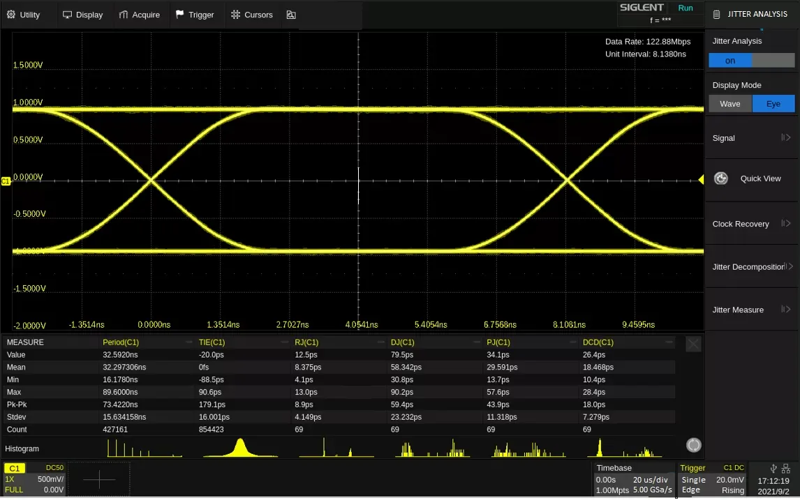
Jitter: Timing variations that reduce the eye diagram's opening, critical for standards like USB 4.0 (20 Gbps).
-
Ground Bounce: Voltage fluctuations in ground planes due to simultaneous switching, impacting signal stability.
-
Delay: Signal propagation delays, influenced by trace length and dielectric constant, affecting timing margins in high-speed protocols.
Addressing these issues requires precise measurement and analysis, which is where specialized SI testing tools come in.
Essential Tools for Signal Integrity Testing
To validate high-speed PCBs, engineers rely on a combination of hardware and software tools. Below, we explore the most effective tools, their applications, and how they help diagnose SI issues.
1. Oscilloscopes for Real-Time Signal Analysis
High-performance oscilloscopes are the cornerstone of SI testing, capturing real-time waveforms to analyze signal behavior. Modern oscilloscopes, like the Keysight UXR-Series or Rohde & Schwarz R&S®RTP, offer bandwidths up to 110 GHz and sample rates exceeding 256 GS/s, making them ideal for multi-gigabit signals.
-
Applications: Measure jitter, rise/fall times, and eye diagrams. For example, a 13 GHz Keysight UXR0134A can generate real-time eye diagrams to assess signal quality for PCIe 6.0 (32 GT/s).
-
Key Features: Advanced equalization modeling (DFE, FFE, CTLE) and eye diagram analysis software to diagnose jitter sources.
-
Practical Tip: Use differential probes for accurate measurements of high-speed differential pairs, ensuring minimal probe loading (e.g., <1 pF capacitance).
2. Vector Network Analyzers (VNAs) for Frequency-Domain Analysis
Vector network analyzers, such as the Rohde & Schwarz R&S®ZNB or Keysight E5080B, measure S-parameters (scattering parameters) to characterize PCB traces, connectors, and vias in the frequency domain. They're essential for validating impedance and insertion loss.
-
Applications: Calculate insertion loss per inch (e.g., 0.5 dB/inch at 10 GHz for FR-4) and detect impedance mismatches. VNAs are replacing traditional time-domain reflectometry (TDR) due to their higher accuracy.
-
Key Features: Multi-port measurements for complex PCB layouts and support for frequencies up to 67 GHz.
-
Practical Tip: Use de-embedding techniques to isolate the device under test (DUT) from fixture effects, ensuring accurate S-parameter measurements.
3. Time-Domain Reflectometry (TDR) Systems
TDR systems, like the R&S®RTP with Option K130, send fast pulses through PCB traces to measure reflections, identifying impedance discontinuities. They're particularly useful for debugging signal paths.
-
Applications: Characterize trace impedance (e.g., ensuring 50 ohms ±5%) and locate faults like via stubs, which can cause reflections at 5 GHz.
-
Key Features: Displays impedance or reflection coefficients over time or distance, aiding in fault localization.
-
Practical Tip: Combine TDR with simulation software to correlate measured reflections with PCB layout issues.
4. Signal Integrity Simulation Software
Simulation tools like Cadence Sigrity, Ansys SIwave, and Altium Designer allow engineers to model SI before fabrication, reducing costly respins. These tools simulate crosstalk, reflections, and power integrity issues using IBIS or SPICE models.
-
Applications: Perform pre-layout analysis to optimize trace widths (e.g., 5 mils for 50-ohm single-ended traces) and post-layout verification of eye diagrams.
-
Key Features: Integration with PCB design platforms for seamless workflow and 3D electromagnetic modeling for EMI analysis.
-
Practical Tip: Use validated IBIS models for accurate buffer behavior, especially for high-speed interfaces like DDR5 (4800 MT/s).
5. Bit Error Rate Testers (BERTs)
BERTs, such as Keysight's M8040A, quantify the performance of digital signals by measuring bit error rates under various conditions. They're critical for validating high-speed serial links.
-
Applications: Test BER for standards like Ethernet (100 Gbps) or USB 4.0, ensuring compliance with specifications (e.g., BER < 10^-12).
-
Key Features: High-speed pattern generators and error detectors for stress testing.
-
Practical Tip: Simulate worst-case scenarios (e.g., maximum cable length) to ensure robust performance.
Best Practices for Effective Signal Integrity Testing
To maximize the effectiveness of these tools, follow these best practices:
-
Define SI Requirements Early: Specify data rates, impedance tolerances, and noise margins based on standards (e.g., 100 ohms ±10% for USB-C differential pairs).
-
Combine Hardware and Software: Use oscilloscopes and VNAs for measurements, complemented by simulations to predict and verify results.
-
Test Under Realistic Conditions: Evaluate PCBs under varying temperatures and loads to mimic real-world operation.
-
Iterate and Optimize: Use test results to refine PCB stackup, routing, and component placement, minimizing SI issues before final fabrication.
How ALLPCB Supports Signal Integrity Validation
At ALLPCB, we empower engineers to achieve superior signal integrity through our advanced manufacturing and rapid prototyping services. Our quick-turn PCB fabrication delivers prototypes in as little as 24 hours, allowing you to test and iterate designs swiftly. With precise control over stackup configurations and high-quality materials, we ensure your PCBs meet stringent impedance and signal quality requirements. Our global logistics network guarantees fast delivery, so you can validate high-speed designs without delay, keeping your projects on schedule and within budget.
Conclusion
Signal integrity testing is the backbone of reliable high-speed PCB design, ensuring signals remain clean and robust at multi-gigabit speeds. By leveraging tools like oscilloscopes, VNAs, TDR systems, simulation software, and BERTs, engineers can diagnose and resolve SI issues with precision. At ALLPCB, we're committed to supporting your success with manufacturing solutions tailored to high-speed applications. Equip yourself with the right tools, follow best practices, and partner with a trusted PCB provider to bring your designs to life with confidence.


