ALLPCB


In the fast-evolving world of electronics, the quality of printed circuit boards (PCBs) plays a crucial role in ensuring reliable performance. One of the most innovative methods to enhance PCB quality is through advanced laser drilling techniques. These techniques directly impact critical aspects such as plating quality, hole wall roughness, debris removal, desmear processes, and drilling accuracy. At ALLPCB, we are committed to leveraging cutting-edge technology to deliver superior PCB solutions. In this blog, we’ll explore how laser drilling transforms PCB manufacturing and why it’s a game-changer for achieving high-quality results.
Why Laser Drilling Matters for PCB Quality
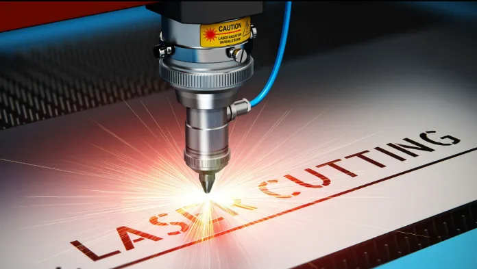
Laser drilling has emerged as a preferred method in PCB manufacturing due to its precision and ability to handle complex designs. Unlike traditional mechanical drilling, laser drilling uses focused beams of energy to create vias and holes with exceptional accuracy. This technology addresses common challenges in PCB production, ensuring better electrical performance and durability. Let’s dive into the specific ways laser drilling improves key areas of PCB quality, including plating quality, hole wall smoothness, debris management, desmear efficiency, and drilling precision.
What is Laser Drilling in PCB Manufacturing?
Laser drilling is a non-contact process that uses a high-energy laser beam to create holes and vias in PCB substrates. This method is especially useful for producing microvias—tiny holes with diameters often less than 0.15 mm—that are essential for high-density interconnect (HDI) boards. The laser’s precision allows for consistent hole shapes and sizes, which are critical for maintaining signal integrity in modern electronics. By eliminating the physical wear associated with mechanical drills, laser drilling also reduces the risk of damage to delicate materials.
Laser Drilling and Plating Quality: Ensuring Reliable Connections
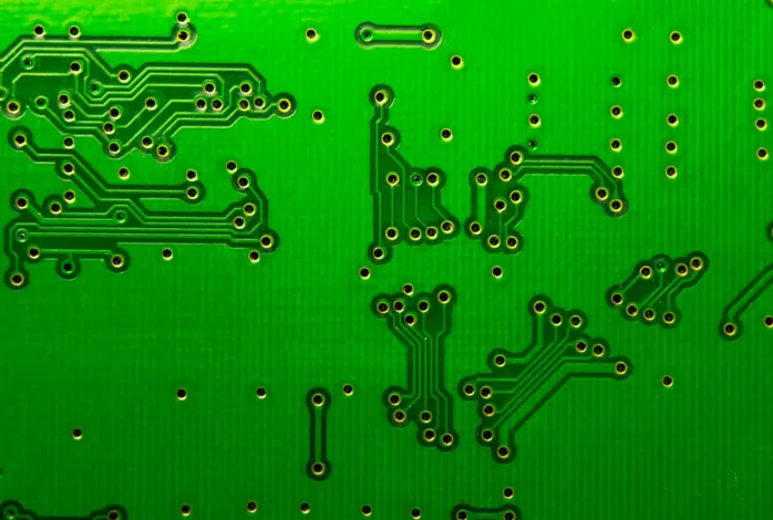
One of the standout benefits of laser drilling is its impact on laser drilling plating quality. Plating is the process of depositing a conductive layer, usually copper, inside the drilled holes to create electrical connections between layers. For plating to be effective, the hole walls must be smooth and free of irregularities. Laser drilling produces cleaner and more uniform holes compared to mechanical methods, which often leave burrs or uneven surfaces. This uniformity allows for a consistent copper layer, reducing the risk of weak connections or signal loss.
In practical terms, better plating quality means improved conductivity and reliability. For example, in high-frequency applications, a poorly plated via can cause signal reflection, leading to impedance mismatches. With laser-drilled holes, the plating process achieves a more even thickness—often within a tolerance of ±0.002 mm—ensuring stable electrical performance. This precision is vital for industries like telecommunications and aerospace, where reliability is non-negotiable.
Reducing Hole Wall Roughness with Laser Drilling
Another critical area where laser drilling excels is in minimizing laser drilling hole wall roughness. Hole wall roughness refers to the texture of the inner surface of a drilled hole. Rough surfaces can trap debris, hinder plating adhesion, and even cause micro-cracks that compromise the PCB’s structural integrity. Mechanical drilling often results in rougher walls due to the physical cutting action, whereas laser drilling vaporizes material with minimal mechanical stress, leaving smoother surfaces.
Smoother hole walls contribute to better long-term performance. For instance, in a study of HDI boards, laser-drilled vias showed a surface roughness reduction of up to 30% compared to mechanically drilled holes. This improvement translates to fewer defects during plating and a lower chance of failure under thermal or mechanical stress. For engineers designing compact, high-performance devices, this level of quality control is invaluable.
Efficient Debris Removal with Laser Drilling
Debris management is a significant concern in PCB drilling, and laser technology offers superior solutions for laser drilling debris removal. During mechanical drilling, bits of substrate material and resin can accumulate inside holes or on the board surface, leading to contamination. If not properly removed, this debris can interfere with plating or cause short circuits. Laser drilling, on the other hand, vaporizes material rather than cutting it, significantly reducing the amount of debris generated.
Additionally, laser systems often incorporate advanced suction or air-blow mechanisms to clear any residual particles during the drilling process. This results in cleaner holes and a reduced need for secondary cleaning steps, saving time and cost in production. For high-volume manufacturing, where even minor defects can lead to significant losses, effective debris removal is a key advantage of laser technology.
Laser Drilling Desmear: Enhancing Hole Cleanliness
Closely related to debris removal is the process of desmearing, and laser drilling offers unique benefits in laser drilling desmear. Desmearing is the removal of smear—a thin layer of melted resin or substrate material that can coat hole walls after drilling. Smear can prevent proper plating adhesion, leading to unreliable electrical connections. While mechanical drilling often requires chemical or plasma desmearing as a separate step, laser drilling minimizes smear formation in the first place due to its controlled energy delivery.
In cases where smear does occur, laser drilling creates holes with consistent geometry, making any subsequent desmearing process more effective. For example, in multilayer PCBs, where vias connect multiple layers, laser-drilled holes ensure that desmearing chemicals can penetrate evenly, achieving a cleaner surface. This leads to better interlayer connectivity and reduces the risk of open circuits, especially in boards with complex stack-ups.
Improving Laser Drilling Accuracy for Precision Designs
Accuracy is at the heart of modern PCB design, and improving laser drilling accuracy is a top priority for manufacturers. Laser drilling systems are capable of creating holes with diameters as small as 0.05 mm, with positional accuracy within ±0.01 mm. This level of precision is essential for HDI and ultra-HDI boards, where space is limited, and components are densely packed. In contrast, mechanical drilling struggles to achieve such tight tolerances, often leading to misalignment or oversized holes.
High accuracy also means better signal integrity. In high-speed digital circuits, for instance, via placement directly affects signal propagation. A deviation of even 0.02 mm can introduce delays or crosstalk, impacting performance. Laser drilling ensures that vias are placed exactly where they are needed, supporting faster signal speeds—often exceeding 10 Gbps in advanced designs. For engineers working on cutting-edge applications, this precision is a critical factor in meeting design specifications.
Advantages of Laser Drilling Over Traditional Methods
Beyond the specific improvements in plating quality, hole wall roughness, debris removal, desmear, and accuracy, laser drilling offers several overarching benefits for PCB manufacturing:
- Non-Contact Process: Since there’s no physical tool involved, there’s no wear or breakage, leading to consistent results over long production runs.
- Versatility: Laser systems can drill a wide range of materials, from standard FR-4 to advanced substrates like polyimide, without needing tool changes.
- Speed: For microvias, laser drilling is often faster than mechanical methods, especially in high-density designs requiring thousands of holes.
- Reduced Thermal Damage: Modern laser systems, such as UV or CO2 lasers, are tuned to minimize heat-affected zones, preserving the integrity of surrounding material.
These advantages make laser drilling an ideal choice for manufacturers aiming to produce high-quality PCBs that meet the demands of today’s technology-driven world.
Applications of Laser Drilling in High-Quality PCB Production
The benefits of laser drilling are particularly evident in specific applications where PCB quality cannot be compromised. Some key areas include:
- Consumer Electronics: Smartphones, tablets, and wearables rely on HDI boards with microvias for compact, efficient designs.
- Automotive Systems: Advanced driver-assistance systems (ADAS) and electric vehicle controls require reliable PCBs with precise vias for safety and performance.
- Medical Devices: Equipment like pacemakers and diagnostic tools demand flawless electrical connections, which laser drilling ensures through superior plating and accuracy.
- Telecommunications: High-frequency boards for 5G infrastructure benefit from the signal integrity provided by laser-drilled vias.
In each of these fields, the ability to produce clean, accurate, and reliable holes directly impacts the end product’s success.
Challenges and Solutions in Laser Drilling for PCBs
While laser drilling offers numerous advantages, it’s not without challenges. Understanding these issues and their solutions can help manufacturers optimize the process:
- Cost: Laser drilling equipment is more expensive than traditional mechanical systems. However, the reduction in defects and secondary processes often offsets the initial investment.
- Material Limitations: Certain materials may absorb laser energy poorly or produce excessive heat. Using the right laser type (e.g., UV for finer control) and adjusting parameters can mitigate this issue.
- Process Complexity: Laser drilling requires precise calibration to avoid over-drilling or under-drilling. Advanced software and automated systems help maintain consistency across large batches.
By addressing these challenges, manufacturers can fully harness the potential of laser drilling to elevate PCB quality.
Conclusion: The Future of PCB Quality with Laser Drilling
Laser drilling is revolutionizing PCB manufacturing by addressing critical quality factors such as laser drilling plating quality, laser drilling hole wall roughness, laser drilling debris removal, laser drilling desmear, and improving laser drilling accuracy. Its precision, cleanliness, and versatility make it an indispensable tool for producing high-performance boards that meet the demands of modern electronics. As technology continues to advance, laser drilling will play an even larger role in enabling smaller, faster, and more reliable devices. At ALLPCB, we’re proud to lead the way in adopting these innovations to provide our clients with top-tier PCB solutions.