 ALLPCB


If you're looking to design a 4-layer PCB stackup that ensures signal integrity, reduces noise, and optimizes performance, you're in the right place. A well-planned 4-layer PCB stackup is crucial for modern electronics, balancing cost and functionality. In this guide, we'll walk you through the essentials of 4-layer PCB design, from choosing the right layer structure to practical tips for optimization. Let's dive into the details of creating an efficient PCB layer stackup that meets your project needs.
What Is a 4-Layer PCB Stackup and Why Does It Matter?
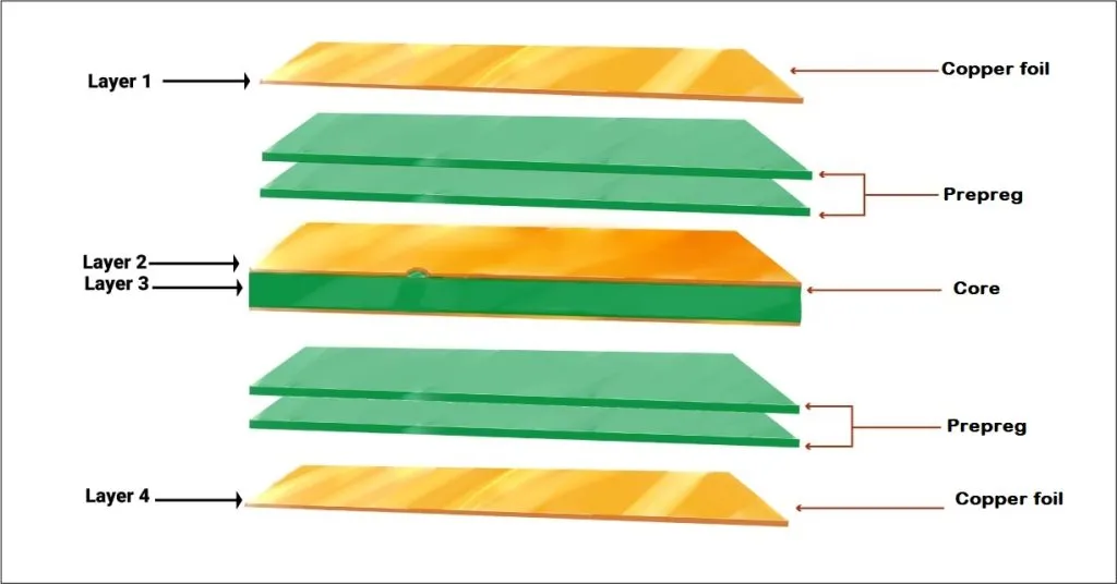
A 4-layer PCB stackup refers to the arrangement of conductive and insulating layers in a printed circuit board with four copper layers. Unlike simpler 2-layer boards, a 4-layer design offers more space for routing signals, power, and ground planes, making it ideal for compact, high-speed, or noise-sensitive applications. The stackup defines how these layers are ordered, typically involving signal layers on the outer surfaces and dedicated power and ground planes in the middle.
Why is optimizing the PCB stackup so important? A poorly designed stackup can lead to issues like electromagnetic interference (EMI), signal crosstalk, and impedance mismatches. For instance, improper spacing between layers can cause signal delays or noise coupling, impacting performance. By carefully planning your 4-layer PCB design, you can minimize these risks, improve signal integrity, and ensure reliable operation even at high frequencies, such as those above 100 MHz commonly seen in digital circuits.
Common 4-Layer PCB Stackup Configurations
When designing a 4-layer PCB, the arrangement of layers plays a critical role in performance. Here are the most common stackup configurations used in 4-layer PCB design, along with their benefits and typical use cases.
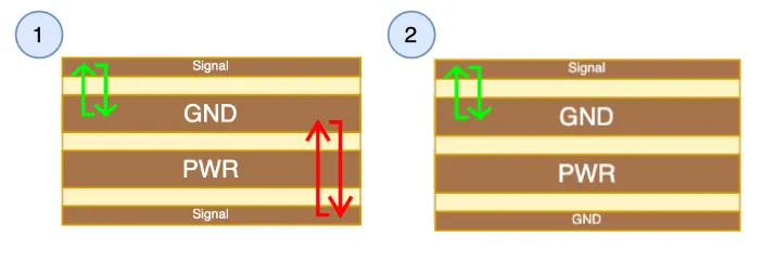
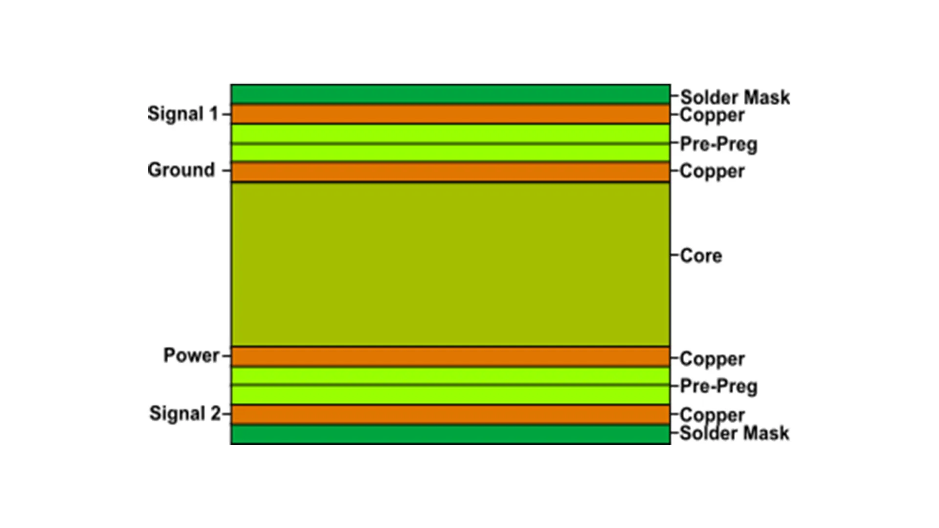
1. Signal-Ground-Power-Signal (SGPS)
This is the most widely used 4-layer PCB stackup. In this setup, the top and bottom layers are dedicated to signal routing, while the inner layers serve as ground (GND) and power (VCC) planes. The ground plane is typically placed on Layer 2, directly beneath the top signal layer, to provide a low-impedance return path for signals and reduce EMI compliance testing.
- Benefits: Excellent signal integrity due to proximity of ground plane to signal layers; effective noise shielding.
- Use Case: High-speed digital circuits, such as microcontrollers or FPGA designs operating at frequencies above 50 MHz.
- Tip: Keep the dielectric thickness between the top signal layer and ground plane small (e.g., 0.2 mm) to maintain tight coupling and control impedance, often targeting 50 ohms for high-speed traces.
2. Signal-Power-Ground-Signal (SPGS)
In this alternative configuration, the power plane is placed on Layer 2, and the ground plane on Layer 3. While this setup is less common, it can be useful when the power plane needs to be closer to specific components on the top layer for better power distribution.
- Benefits: Improved power delivery for top-layer components.
- Use Case: Designs with heavy power requirements on the top layer, such as power amplifiers.
- Tip: Ensure the ground plane still provides a solid return path for bottom-layer signals to avoid noise issues.
Key Factors to Consider in 4-Layer PCB Design
Creating an optimized PCB layer stackup involves more than just picking a configuration. Here are the critical factors to consider during the design process to ensure performance and manufacturability.
1. Layer Thickness and Dielectric Material
The thickness of the dielectric material between layers affects impedance and signal speed. For high-speed designs, a thinner dielectric (e.g., 0.1 to 0.2 mm) between signal and ground layers helps maintain controlled impedance, often targeting 50 or 75 ohms for differential pairs. Standard FR-4 material with a dielectric constant (Dk) of around 4.2 to 4.5 is commonly used, but for higher frequencies (above 1 GHz), consider low-loss materials like Rogers with a Dk of 3.0 to 3.5.
Practical Tip: Use a stackup calculator tool to determine the exact dielectric thickness needed for your target impedance. For example, a 50-ohm trace on a 1.6 mm thick FR-4 board might require a trace width of 0.3 mm with a 0.2 mm dielectric spacing to the ground plane.
2. Power and Ground Plane Integrity
Dedicated power and ground planes are a major advantage of a 4-layer PCB stackup. A solid ground plane reduces noise by providing a consistent return path for signals. Avoid splitting the ground plane unless absolutely necessary, as splits can create loops and increase EMI. Similarly, ensure the power plane is continuous and placed close to the ground plane to form a low-inductance capacitor, reducing power supply noise.
Practical Tip: Place decoupling capacitors (e.g., 0.1 μF) near power pins of ICs to filter noise, connecting them directly to the power and ground planes with short vias.
3. Signal Routing and Trace Placement
In a 4-layer PCB design, signal traces are usually routed on the top and bottom layers. High-speed signals should be routed on the layer closest to the ground plane (typically the top layer in an SGPS stackup) to minimize interference. Keep trace lengths short for critical signals to reduce propagation delay—signals travel at approximately 150 mm/ns on FR-4 material, so a 150 mm trace introduces a 1 ns delay.
Practical Tip: For differential pairs, maintain consistent spacing (e.g., 0.2 mm) and length matching within 0.5 mm to avoid skew in high-speed protocols like USB or HDMI.
Suggested Reading: Why need to know 4 Layer PCB Stack-up Technology?
Optimization Tips for 4-Layer PCB Stackup
Beyond the basics, here are actionable tips to fine-tune your PCB stackup for maximum performance and reliability. These strategies address common challenges in 4-layer PCB design.
1. Minimize Crosstalk with Proper Layer Spacing
Crosstalk occurs when signals on adjacent traces or layers interfere with each other. In a 4-layer PCB, this can happen between top and bottom signal layers if they are too close. Increase the dielectric thickness between signal layers (e.g., to 0.8 mm or more) while keeping the signal-to-ground spacing tight (e.g., 0.2 mm). This reduces coupling between signal layers while maintaining good impedance control.
2. Use Vias Strategically
Vias connect traces between layers, but they can introduce inductance and signal reflections if overused. For high-speed signals, use microvias or blind vias to minimize stub length, and place ground vias near signal vias to provide a return path. Limit via transitions for critical signals to one or two per net to avoid delays.
3. Plan for Thermal Management
In designs with high-power components, heat dissipation can be a concern. Use the power and ground planes to spread heat by connecting thermal vias from hot components to these planes. For example, a power IC dissipating 2W might require 4 to 6 thermal vias of 0.3 mm diameter to transfer heat effectively.
4. Simulate and Test Your Stackup
Before finalizing your 4-layer PCB stackup, use simulation tools to model signal integrity and impedance. Tools can predict issues like ringing or overshoot in high-speed signals, allowing you to adjust layer spacing or trace width. After PCB manufacturing, test the board with an oscilloscope to verify signal quality—look for clean edges with rise times under 1 ns for high-speed signals.
Common Mistakes to Avoid in 4-Layer PCB Stackup Design
Even experienced designers can make errors in PCB layer stackup planning. Here are pitfalls to watch out for:
- Splitting Ground Planes: Breaking the ground plane for routing convenience can create noise loops. Always prioritize a continuous ground plane.
- Ignoring Impedance Control: Failing to calculate trace width and layer spacing for controlled impedance can degrade signal quality, especially at frequencies above 100 MHz.
- Overloading Signal Layers: Routing too many traces on one layer can lead to congestion and crosstalk. Distribute signals evenly between top and bottom layers.
- Poor Via Placement: Placing vias far from ground planes can disrupt return paths, increasing noise. Keep vias close to reference planes.
Applications of 4-Layer PCB Stackup
A well-designed 4-layer PCB stackup is versatile and suits a wide range of applications. Here are a few examples where this configuration shines:
- Consumer Electronics: Smartphones and tablets use 4-layer PCBs to pack high-speed digital signals and power distribution into a compact form.
- Industrial Controls: PLCs and automation systems benefit from noise immunity provided by dedicated ground planes.
- Automotive Systems: ECUs and sensor modules rely on 4-layer designs for reliability in harsh environments.
Suggested Reading: 4 layers PCB: Everything You Need to Know
Conclusion: Building a Better 4-Layer PCB Stackup
Optimizing a 4-layer PCB stackup is a balancing act between signal integrity, noise reduction, and manufacturability. By choosing the right configuration, such as the Signal-Ground-Power-Signal stackup, and paying attention to layer spacing, via placement, and impedance control, you can create a design that performs reliably even in demanding applications. Remember to simulate your design, test prototypes, and avoid common mistakes like splitting ground planes or ignoring thermal needs.
Whether you're working on high-speed digital circuits or power-intensive systems, a carefully planned PCB layer stackup is the foundation of success. Use the tips and strategies in this guide to streamline your 4-layer PCB design process and achieve better results for your next project.


