 ALLPCB


In the fast-evolving world of networking, router and switch PCBs (Printed Circuit Boards) are at the heart of innovation. As data demands grow with the rise of 5G, IoT, and cloud computing, the design and manufacturing of these critical components must keep pace. So, what does the future hold for router and switch PCB trends? This blog dives deep into the latest technologies and advancements, including advanced PCB materials, high density interconnect (HDI), embedded components, and 3D PCB designs, to help engineers and tech enthusiasts stay ahead of the curve.
Whether you're designing cutting-edge networking equipment or simply exploring the future of electronics, this guide will walk you through the key trends and technologies shaping router and switch PCBs. Let’s explore how these innovations are driving performance, efficiency, and reliability in 2025 and beyond.
Why Router and Switch PCBs Are Critical to Networking
Router and switch PCBs form the backbone of modern communication systems. These boards connect components, manage high-speed data transmission, and ensure minimal signal loss in devices that power the internet and enterprise networks. With data traffic expected to grow exponentially—projected to reach 4.8 zettabytes per year by 2025, according to industry forecasts—these PCBs must handle higher frequencies, tighter tolerances, and greater thermal stress.
The push for faster, smaller, and more efficient networking hardware means PCB designers face unique challenges. From maintaining signal integrity at speeds exceeding 25 Gbps to fitting more functionality into compact spaces, the future of these boards lies in groundbreaking materials and design techniques. Let’s break down the top trends driving this transformation.
Trend 1: Advanced PCB Materials for High-Performance Networking
One of the most significant router switch PCB trends is the shift toward advanced materials. Traditional FR-4 laminates, while cost-effective, struggle to meet the demands of high-frequency signals and thermal management in modern routers and switches. New materials are stepping in to address these limitations.
Low-Loss Dielectrics: Materials like PTFE (Polytetrafluoroethylene) and advanced laminates with dielectric constants below 3.0 are becoming popular. These materials reduce signal loss at frequencies above 10 GHz, which is critical for 5G and next-gen Wi-Fi routers. For example, a PTFE-based PCB can achieve a signal loss of less than 0.002 dB/inch at 10 GHz, compared to 0.01 dB/inch for standard FR-4.
High-Thermal-Conductivity Substrates: As routers and switches pack more power into smaller form factors, heat dissipation is a growing concern. Materials with thermal conductivity ratings of 1.5 W/mK or higher, such as ceramic-filled laminates, help manage temperatures and prevent component failure during continuous operation.
Sustainable Options: With environmental regulations tightening, eco-friendly materials like halogen-free laminates are gaining traction. These alternatives reduce toxic emissions during manufacturing while maintaining performance standards for high-speed networking.
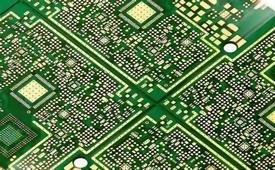
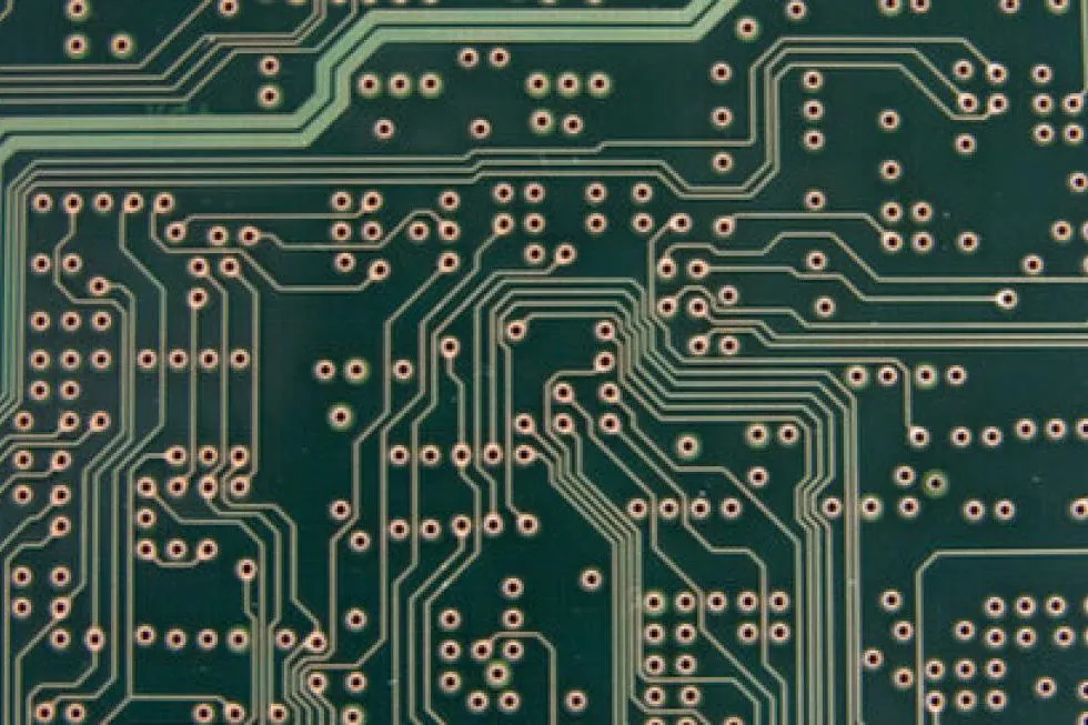
Trend 2: High Density Interconnect (HDI) for Compact and Efficient Designs
High Density Interconnect (HDI) technology is revolutionizing router and switch PCBs by enabling more components to fit into smaller spaces. HDI designs use microvias, blind vias, and buried vias to create denser routing, which is essential for compact networking devices that need to support multiple high-speed connections.
Benefits of HDI: With microvias as small as 0.1 mm in diameter, HDI allows for layer counts exceeding 20 in a single board, reducing the overall footprint. This is particularly useful for edge routers and data center switches where space is at a premium. Additionally, HDI improves signal integrity by shortening trace lengths, minimizing impedance mismatches at speeds up to 56 Gbps.
Challenges: While HDI offers incredible advantages, it requires precision manufacturing techniques and advanced design tools to ensure reliability. For instance, maintaining a consistent aspect ratio of 0.8:1 for microvias is critical to avoid defects during production.
HDI is expected to dominate the market, with industry reports predicting a significant increase in adoption by 2025, driven by the need for miniaturization in networking hardware. This trend aligns perfectly with the growing complexity of multi-port switches and modular routers.
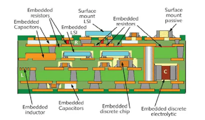
Trend 3: Embedded Components for Enhanced Functionality
Embedding components directly into the PCB substrate is another game-changer for router and switch designs. This technology involves placing passive components like resistors, capacitors, and even active components like ICs within the board layers, rather than mounting them on the surface.
Advantages for Networking: Embedded components reduce the board’s surface area, allowing for sleeker designs in compact routers. They also improve signal performance by minimizing parasitic inductance and capacitance—key factors when dealing with signals at 25 Gbps or higher. For example, embedding a decoupling capacitor near a high-speed processor can reduce noise by up to 30% compared to surface-mounted alternatives.
Applications: In high-end switches used in data centers, embedded components help manage power distribution and signal filtering within a confined space. This trend is particularly relevant as devices move toward multi-functionality, requiring more components without increasing size.
Future Outlook: As manufacturing processes improve, the cost of embedding components is expected to drop, making this technology more accessible for mid-range networking equipment by the end of the decade.
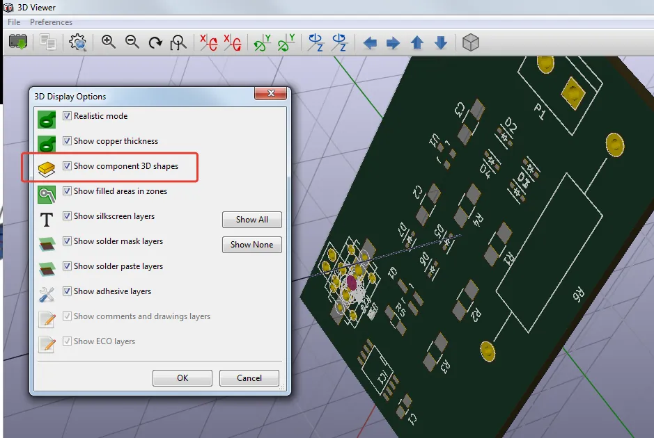
Trend 4: 3D PCB Designs for Next-Gen Router and Switch Architectures
3D PCB design is an emerging trend that takes PCB layouts beyond the traditional flat, two-dimensional structure. By stacking multiple layers or using additive manufacturing techniques, 3D PCBs create three-dimensional circuits that optimize space and performance.
Why 3D PCBs Matter: In routers and switches, where every millimeter counts, 3D designs allow for vertical integration of components. This means more functionality can be packed into a smaller footprint, ideal for portable or modular networking devices. Additionally, 3D structures can reduce signal path lengths, improving latency and supporting speeds beyond 100 Gbps.
Manufacturing Techniques: Additive manufacturing, often referred to as 3D printing for electronics, is making it possible to create complex geometries that traditional subtractive methods can’t achieve. For instance, a 3D-printed PCB can integrate conformal cooling channels to manage heat in high-power switches, maintaining performance under load.
Challenges: While promising, 3D PCB technology is still in its early stages. High costs and limited material options are barriers to widespread adoption. However, as the technology matures, it’s poised to redefine how networking hardware is designed and built.
Trend 5: Integration of AI and Automation in PCB Design
Artificial Intelligence (AI) and automation are not just buzzwords; they’re becoming integral to PCB design for routers and switches. These technologies streamline the design process, optimize layouts, and reduce errors in complex boards.
AI-Driven Design Tools: AI algorithms can analyze signal integrity, thermal performance, and electromagnetic interference (EMI) in real-time, suggesting optimal trace routing for high-speed signals. For example, AI can reduce design iterations by up to 40%, saving time in the development of multi-layer HDI boards for data center switches.
Automation in Manufacturing: Automated assembly lines equipped with machine vision ensure precise placement of microvias and embedded components, critical for maintaining the tight tolerances required in modern networking PCBs. This also lowers production costs and improves scalability for large-volume orders.
The integration of AI and automation is set to accelerate innovation, enabling designers to push the boundaries of what’s possible in router and switch PCB performance.
Trend 6: Sustainability in PCB Manufacturing
Sustainability is no longer optional—it’s a priority in PCB manufacturing. As environmental concerns grow, the industry is adopting greener practices to reduce waste and energy consumption in the production of router and switch PCBs.
Eco-Friendly Materials: Beyond halogen-free laminates, manufacturers are exploring bio-based resins and recyclable substrates to minimize environmental impact. These materials maintain the dielectric and thermal properties needed for high-frequency applications.
Energy-Efficient Processes: Advances in manufacturing, such as low-temperature soldering and water-based cleaning, cut down on energy use and chemical waste. Some facilities report a 20% reduction in carbon footprint by adopting these methods.
For engineers and companies, choosing sustainable PCB solutions not only meets regulatory requirements but also appeals to eco-conscious clients in the networking sector.
How These Trends Benefit Engineers and Designers
For engineers working on router and switch designs, staying updated on these trends offers a competitive edge. Advanced materials ensure your boards can handle the high frequencies of 5G and beyond. HDI and embedded components allow you to create smaller, more powerful devices without sacrificing performance. 3D PCB designs open up new possibilities for innovation, while AI and automation save time and reduce errors in complex projects. Finally, sustainable practices align your work with global environmental goals, enhancing your reputation in the industry.
By adopting these technologies, you can design networking hardware that meets today’s demands and anticipates tomorrow’s challenges. Whether you’re optimizing signal integrity or shrinking board size, these advancements provide the tools to succeed.
Conclusion: Preparing for the Future of Router and Switch PCBs
The future of router and switch PCBs is bright, driven by incredible advancements in materials, design techniques, and manufacturing processes. From advanced PCB materials that tackle high-frequency challenges to HDI and embedded components that enable compact designs, these trends are transforming how networking hardware performs. 3D PCB designs and AI-driven tools are pushing the boundaries of innovation, while sustainability ensures the industry moves forward responsibly.
As data demands continue to soar, staying ahead of these router switch PCB trends is essential for engineers and designers. By embracing these technologies, you can create networking solutions that are faster, smaller, and more reliable—ready for the challenges of 2025 and beyond. Keep exploring, keep innovating, and let these advancements guide your next project to success.


