 ALLPCB


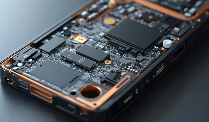
In the fast-paced world of mobile technology, Printed Circuit Boards (PCBs) are the backbone of every device, connecting components and enabling functionality. As smartphones continue to evolve, so do the PCBs that power them. What does the future hold for mobile phone PCBs? Emerging trends like embedded components, 3D PCBs, flexible electronics, and advanced materials are shaping the next generation of mobile devices, promising smaller, faster, and more efficient designs.
In this blog, we’ll dive deep into the future of PCBs, exploring the innovations driving mobile phone technology forward. From the integration of embedded components to the rise of flexible electronics, we’ll break down the key advancements and what they mean for engineers and manufacturers. Let’s explore how these trends are redefining the landscape of mobile phone design and production.
Why Mobile Phone PCBs Are Evolving Rapidly
Mobile phones are no longer just communication tools; they’re powerful mini-computers packed with features like high-resolution cameras, AI processors, and 5G connectivity. This demand for more functionality in smaller devices is pushing PCB technology to new limits. Engineers are tasked with designing boards that can handle higher signal speeds—often exceeding 10 Gbps for 5G applications—while maintaining low impedance, typically below 50 ohms for optimal performance.
The drive for slimmer phones also means PCBs must shrink without losing efficiency. Traditional rigid boards are giving way to innovative designs that save space and improve performance. Additionally, sustainability is becoming a priority, with manufacturers seeking eco-friendly materials and processes. These challenges are fueling groundbreaking trends in PCB technology, which we’ll explore in detail below.
Trend 1: Embedded Components in Mobile Phone PCBs
One of the most exciting developments in the future of PCBs is the use of embedded components. This technology involves placing active and passive components—such as resistors, capacitors, and even microchips—directly inside the PCB substrate, rather than mounting them on the surface. For mobile phones, this means significant space savings, allowing for thinner designs or more room for other features like larger batteries.
Embedded components also improve performance by reducing the distance between elements, which lowers parasitic inductance and enhances signal integrity. For instance, in high-frequency applications like 5G, signal speeds can reach up to 25 Gbps, and minimizing interference is critical. By embedding components, manufacturers can achieve impedance values as low as 25 ohms in certain layers, optimizing data transfer.
Beyond performance, this trend reduces assembly costs and enhances reliability since there are fewer solder joints that could fail. As mobile devices continue to demand more compact and efficient designs, embedded components are set to become a standard in PCB manufacturing.
Trend 2: The Rise of 3D PCBs for Compact Designs
Another game-changer in mobile phone technology is the adoption of 3D PCBs. Unlike traditional flat boards, 3D PCBs are structured in multiple layers or even folded configurations, allowing for a higher density of components in a smaller footprint. This is particularly important for smartphones, where every millimeter of space counts.
With 3D PCBs, manufacturers can stack circuits vertically, reducing the overall board size while increasing functionality. This technology also supports better thermal management, as heat can be dissipated more evenly across layers. For example, in a typical smartphone PCB, power dissipation can reach 5 watts or more during heavy usage, and 3D designs help prevent overheating by spreading thermal load.
This innovation is paving the way for futuristic phone designs, including foldable devices where the PCB itself can conform to unique shapes. As 3D printing technology advances, we’re also seeing the potential for fully printed 3D circuits, which could further streamline production and customization.
Trend 3: Flexible Electronics Transforming Mobile Devices
Flexible electronics are revolutionizing the way mobile phones are designed and used. These PCBs are made from bendable materials like polyimide, allowing them to curve or fold without breaking. This technology is at the heart of foldable smartphones, which are becoming increasingly popular as consumers seek larger screens in portable formats.
Flexible PCBs offer more than just adaptability; they also reduce weight and improve durability. Traditional rigid boards can crack under stress, but flexible electronics can withstand repeated bending—often up to 100,000 cycles in testing—making them ideal for innovative designs. They also enable better integration with other flexible components, such as OLED displays, which require signal speeds of around 1 Gbps for smooth performance.
As the demand for wearable technology grows, flexible electronics will play a larger role in mobile phone ecosystems, connecting devices like smartwatches and fitness trackers. This trend highlights the importance of lightweight, adaptable materials in the future of PCBs, ensuring that mobile devices remain both functional and user-friendly.
Trend 4: Advanced Materials Driving PCB Innovation
The materials used in PCB manufacturing are evolving to meet the needs of modern mobile phones. Advanced materials are being developed to handle higher frequencies, reduce signal loss, and improve thermal performance. For instance, low-loss laminates are now commonly used in 5G-enabled devices to support frequencies above 6 GHz with dielectric constants as low as 2.2, minimizing signal degradation.
Another promising area is the use of eco-friendly substrates. With growing environmental concerns, manufacturers are exploring biodegradable materials like cellulose-based composites for PCB production. These materials not only reduce electronic waste but also maintain decent performance, with thermal conductivity values around 0.5 W/mK, suitable for low-power mobile applications.
Graphene and other nanomaterials are also on the horizon, offering incredible conductivity and strength. While still in the research phase for widespread PCB use, graphene could potentially achieve electrical conductivity up to 10^8 S/m, far surpassing traditional copper traces. These advanced materials are set to redefine the efficiency and sustainability of mobile phone PCBs in the coming years.

Trend 5: Miniaturization and High-Density Interconnects (HDI)
Miniaturization remains a core focus in mobile phone PCB design, driven by High-Density Interconnect (HDI) technology. HDI PCBs use finer traces—often as narrow as 50 micrometers—and smaller vias to pack more components into a limited space. This is essential for modern smartphones, which may house over 1,000 components on a single board smaller than 100 square centimeters.
HDI technology also supports faster signal transmission by reducing the length of interconnects, which is crucial for maintaining signal integrity at speeds above 10 Gbps. Additionally, it allows for better power distribution, with current densities often reaching 10 A/cm2 in critical areas, ensuring stable performance even in compact designs.
As mobile devices continue to integrate more features like augmented reality and advanced sensors, HDI will be key to balancing size constraints with performance demands. This trend underscores the ongoing push for smaller, yet more powerful, PCB solutions in the mobile industry.
The Impact of These Trends on Mobile Phone Manufacturing
The innovations in PCB technology are transforming every aspect of mobile phone manufacturing. Embedded components and 3D PCBs are streamlining assembly processes by reducing the number of separate parts and soldering steps, which can cut production time by up to 20% in some cases. Flexible electronics are enabling entirely new product categories, like foldable phones, while also improving durability and reducing repair costs.
Advanced materials and HDI designs are enhancing performance, allowing phones to support cutting-edge features like 5G and AI without increasing size or power consumption. For engineers, these trends mean new design challenges but also exciting opportunities to push the boundaries of what’s possible in mobile technology.
From a sustainability standpoint, the shift toward biodegradable materials and efficient designs is helping manufacturers reduce their environmental footprint. As these technologies mature, we can expect mobile phones to become not only more powerful but also more eco-conscious.
Challenges and Opportunities in Adopting New PCB Technologies
While the future of PCBs is bright, there are hurdles to overcome. Implementing embedded components and 3D designs requires advanced manufacturing equipment and expertise, which can increase upfront costs. For instance, embedding components often demands precision drilling and lamination processes with tolerances below 10 micrometers, a significant investment for many facilities.
Flexible electronics, while promising, face challenges in mass production due to the complexity of ensuring consistent quality across bendable substrates. Advanced materials like graphene are still expensive and not yet viable for widespread use, with production costs potentially 10 times higher than traditional copper.
However, these challenges also present opportunities. Companies that invest in cutting-edge PCB technologies can gain a competitive edge by offering innovative, high-performance mobile solutions. Collaboration between material scientists, engineers, and manufacturers will be crucial to overcoming these barriers and bringing the future of PCBs to reality.
How to Prepare for the Future of Mobile Phone PCBs
For engineers and manufacturers, staying ahead of these trends means adapting to new tools and processes. Investing in design software that supports 3D modeling and HDI layouts is a good starting point. Training teams on the intricacies of embedding components and working with flexible substrates will also be essential for seamless integration into production lines.
Partnering with a reliable PCB provider that embraces innovation can make a big difference. Look for services that offer expertise in advanced materials and cutting-edge manufacturing techniques to ensure your mobile phone designs are future-ready. Keeping an eye on industry developments, such as the adoption of sustainable materials, can also help align your projects with emerging market demands.
Conclusion: Shaping the Future of Mobile Technology
The future of mobile phone PCBs is full of exciting possibilities, from embedded components and 3D PCBs to flexible electronics and advanced materials. These trends are not just improving performance but also enabling entirely new types of devices that are smaller, more powerful, and more sustainable. As technology continues to advance, staying informed about these innovations will be key for anyone involved in mobile phone design and manufacturing.
At ALLPCB, we’re committed to supporting engineers and manufacturers in navigating this evolving landscape. By leveraging the latest in PCB technology, we aim to help bring your mobile device concepts to life with precision and efficiency. The future of PCBs is here, and it’s set to redefine how we connect and communicate in the years ahead.


