 ALLPCB


For PCB designers looking to optimize space, enhance signal integrity, and reduce costs in multilayer designs, mastering blind vias is essential. Blind vias connect internal layers of a printed circuit board (PCB) without extending through the entire board, offering unique advantages in high-density interconnect (HDI) designs. In this guide, we’ll cover blind via PCB design rules, blind via design for manufacturability, a step-by-step Altium blind via tutorial, and blind via best practices to help you create efficient and reliable PCB layouts.
Whether you're a beginner or an experienced designer, this comprehensive blog will provide actionable insights, specific examples, and technical details to elevate your PCB design skills. Let’s be with ALLPCB to dive into the world of blind vias and explore how to implement them effectively in your projects.
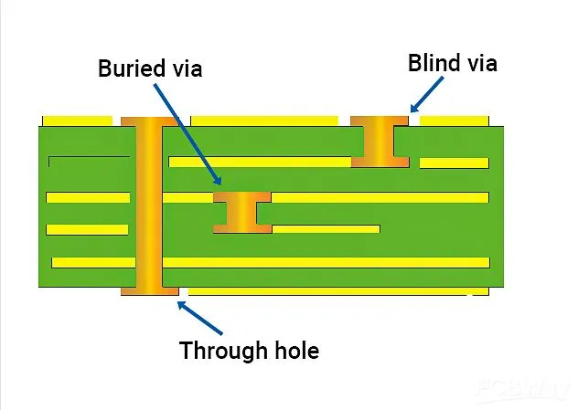
What Are Blind Vias and Why Do They Matter?
Blind vias are a type of via in PCB design that connect two or more internal layers of a multilayer board without penetrating through to the external layers. Unlike through-hole vias, which go all the way through the board, blind vias are drilled and plated only to a certain depth, making them “invisible” from one side of the board.
The importance of blind vias lies in their ability to save space and improve design efficiency. By stacking vias in the vertical (z-axis) direction, they free up valuable surface area for components and traces. Additionally, they can enhance signal integrity by reducing trace lengths, which lowers inductance and minimizes signal loss. For example, in high-speed designs, shorter connections via blind vias can reduce signal propagation delay, often by as much as 20-30% compared to traditional through-hole vias in some configurations.
In terms of cost, blind vias can also eliminate the need for complex through-hole plating processes, potentially reducing manufacturing expenses by 10-15% in HDI designs. However, to fully leverage these benefits, designers must adhere to specific design rules and manufacturing constraints. Let’s explore these in detail.
Blind Via PCB Design Rules: Key Guidelines to Follow
Designing with blind vias requires careful attention to specific rules to ensure functionality and manufacturability. Below are the critical blind via PCB design rules every designer should follow:
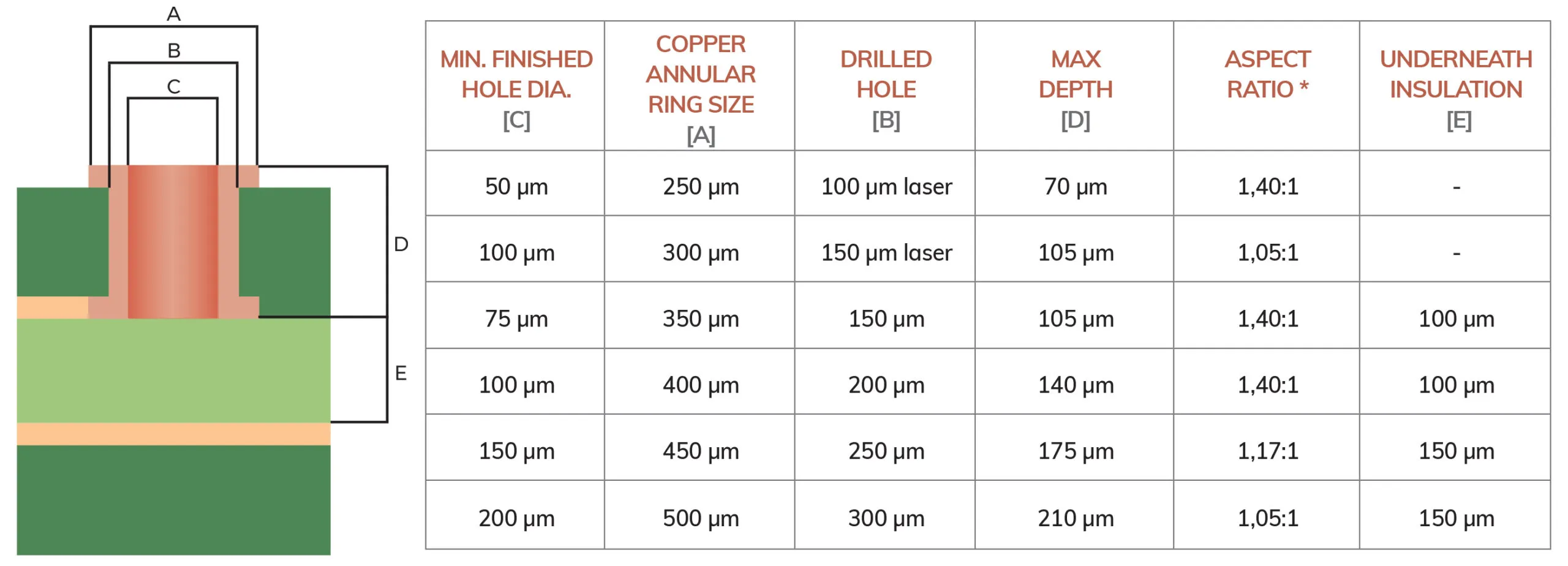
- Aspect Ratio Constraints: The aspect ratio of a blind via (depth to diameter) is crucial for reliable plating and drilling. Most manufacturers recommend an aspect ratio of 1:1 or lower for blind vias. For instance, a via with a diameter of 0.2 mm should not exceed a depth of 0.2 mm to avoid plating issues.
- Minimum Drill Size: Blind vias often require smaller drill sizes compared to through-hole vias. A typical minimum drill size for blind vias is 0.15 mm (6 mils), though this can vary based on the manufacturer’s capabilities.
- Layer Stack-Up Planning: Blind vias must be planned according to the layer stack-up. They should connect only the intended layers without interfering with others. For a 6-layer board, a blind via might connect layers 1 to 2 or 2 to 3, but not beyond.
- Clearance and Spacing: Ensure adequate spacing between blind vias and other board features like traces and pads. A common rule is to maintain a clearance of at least 0.2 mm (8 mils) to prevent shorts or manufacturing defects.
- Signal Integrity Considerations: For high-speed designs operating at frequencies above 1 GHz, blind vias can help reduce stub effects that degrade signal quality. Position them to minimize impedance mismatches, ideally maintaining a characteristic impedance of 50 ohms for most RF applications.
Adhering to these rules ensures that your design is not only functional but also manufacturable. Ignoring them can lead to issues like incomplete plating, drilling inaccuracies, or signal degradation.
Blind Via Design for Manufacturability: Tips for Success
Designing blind vias with manufacturability in mind is critical to avoid costly revisions and production delays. Here are essential tips for blind via design for manufacturability:
- Consult Manufacturer Guidelines Early: Different fabrication houses have varying capabilities for blind via drilling and plating. Some may support microvias down to 0.1 mm (4 mils), while others are limited to 0.2 mm (8 mils). Always check these specs before finalizing your design.
- Limit Via Stacking Complexity: While stacking blind vias can save space, excessive stacking (more than two sequential vias) can complicate manufacturing and increase costs by up to 25%. Use stacked vias only when necessary.
- Optimize Via Depth Control: Blind vias require precise depth control during drilling. Laser drilling is often used for microvias to achieve accuracies within ±0.025 mm. Ensure your design specifies via depths that align with these tolerances.
- Avoid Overlapping Vias: Overlapping blind vias on different layer pairs can cause structural weaknesses in the board. Maintain a minimum offset of 0.3 mm (12 mils) between vias on adjacent layer pairs.
- Material Selection: Choose materials compatible with blind via processes. For example, high-Tg FR-4 materials (with a glass transition temperature above 170°C) are often preferred for HDI PCBs to withstand the thermal stresses of microvia laser drilling.
By focusing on these manufacturability aspects, you can reduce the risk of production errors and ensure a smoother transition from design to fabrication.

Altium Blind Via Tutorial: Step-by-Step Implementation
For designers using popular PCB design software, setting up blind vias can be straightforward with the right steps. This Altium blind via tutorial will guide you through the process of creating and configuring blind vias in your projects.
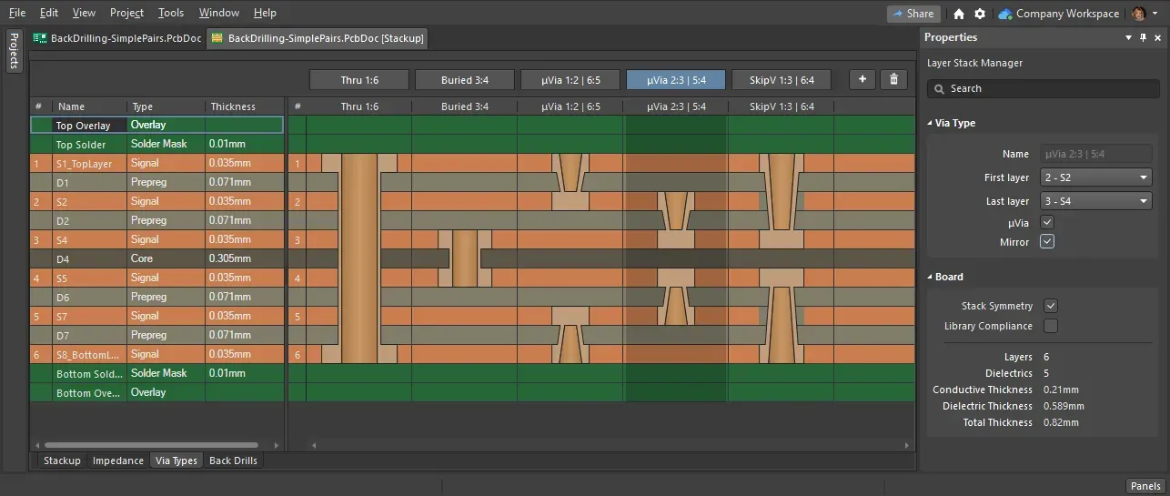
- Define the Layer Stack: Start by opening the Layer Stack Manager in your design software. Define the number of layers and their connections. For instance, in a 6-layer board, you might set blind vias to connect layers 1-2 and 5-6.
- Set Via Types: In the via properties panel, select “Blind” as the via type. Specify the start and stop layers for each blind via. For example, a via connecting layers 1 to 2 should have a start layer of 1 and a stop layer of 2.
- Adjust Via Dimensions: Set the via diameter and drill size according to your design rules. A common setting for blind vias is a diameter of 0.3 mm (12 mils) with a drill size of 0.2 mm (8 mils).
- Place the Via: Use the via placement tool to position the blind via in your layout. Ensure it aligns with the nets connecting the specified layers. The software will automatically restrict the via to the defined layer range.
- Verify Design Rules: Run a design rule check (DRC) to confirm that the blind via meets clearance, spacing, and manufacturability constraints. Adjust as needed to resolve any violations.
- Generate Manufacturing Outputs: When exporting Gerber files or drill data, ensure that the blind via specifications are clearly indicated. Include a fabrication note specifying the via type and layer connections for clarity.
Following these steps ensures that blind vias are correctly implemented in your design tool, minimizing errors during fabrication. Always double-check the output files to confirm that the blind via data is accurately represented.
Blind Via Best Practices: Maximizing Performance and Reliability
To achieve optimal results with blind vias, follow these blind via best practices tailored for performance, reliability, and ease of manufacturing:
- Use Blind Vias for High-Density Areas: Reserve blind vias for areas of your board where space is at a premium, such as under BGA (Ball Grid Array) components with pitches as tight as 0.5 mm. This allows for efficient routing without sacrificing board real estate.
- Balance Cost and Complexity: While blind vias can reduce costs by eliminating through-hole plating, they can increase expenses if overused or improperly designed. Aim for a balance by using them only where necessary, typically in designs with 6 or more layers.
- Simulate Signal Performance: For high-speed applications, use simulation tools to analyze the impact of blind vias on signal integrity. Ensure that return loss remains below -15 dB and insertion loss is minimized, especially for frequencies above 5 GHz.
- Collaborate with Fabricators: Early collaboration with your fabrication partner can prevent design issues. Share your layer stack-up and via specifications to confirm that they align with the manufacturer’s capabilities, reducing the risk of delays.
- Test Prototypes Thoroughly: After fabrication, test prototypes for electrical continuity and signal performance. Use tools like a Time-Domain Reflectometer (TDR) to verify that blind vias maintain impedance control, ideally within ±10% of the target value (e.g., 50 ohms).
Implementing these best practices will help you create robust PCB designs that meet both performance and manufacturing requirements.
Common Challenges with Blind Vias and How to Overcome Them
While blind vias offer numerous benefits, they also come with challenges that designers must address. Here are some common issues and solutions:
- Drilling Accuracy: Inaccurate drilling depth can lead to incomplete connections. Solution: Use laser drilling for microvias and specify tight tolerances (e.g., ±0.025 mm) in your design files.
- Plating Issues: Poor plating in blind vias can cause open circuits. Solution: Maintain a low aspect ratio (1:1 or less) and work with manufacturers who use advanced plating techniques like reverse pulse plating.
- Cost Overruns: Complex blind via designs can increase PCB manufacturing costs. Solution: Limit the number of blind via sequences and optimize their placement to reduce manufacturing complexity.
- Signal Stub Effects: Unused portions of vias can act as stubs, degrading signal quality. Solution: Design blind vias to terminate at the exact layer needed, avoiding unnecessary extensions.
By anticipating these challenges and applying the suggested solutions, you can mitigate risks and ensure a successful design outcome.
Conclusion: Elevate Your PCB Designs with Blind Vias
Blind vias are a powerful tool for PCB designers, offering space savings, improved signal integrity, and cost efficiencies in multilayer and HDI designs. By following the blind via PCB design rules, focusing on blind via design for manufacturability, leveraging tools as outlined in our Altium blind via tutorial, and adhering to blind via best practices, you can create high-performing, reliable boards that meet modern design demands.
Start integrating blind vias into your next project with confidence. Use the guidelines and tips provided in this guide to navigate the complexities of design and manufacturing, ensuring that your PCBs are both innovative and practical. With careful planning and execution, blind vias can transform your approach to PCB layout, opening up new possibilities for compact, high-speed designs.


