 ALLPCB


In the fast-evolving world of printed circuit board (PCB) manufacturing, precision and efficiency are critical to meeting the demands of modern electronics. Drilling, a foundational step in PCB fabrication, creates the holes necessary for vias, component leads, and mechanical mounting. Two primary methods dominate this process: mechanical drilling and laser drilling. Each offers distinct advantages and trade-offs, making the choice between them pivotal for engineers designing high-performance PCBs. In this blog, we dive deep into both techniques, comparing their capabilities, limitations, and applications to help you decide which is best for your project.
Whether you're working on high-density interconnect (HDI) boards for smartphones or robust multilayer PCBs for automotive systems, understanding the nuances of these drilling methods can optimize your design and manufacturing process. Let's explore the key differences, backed by technical insights and practical examples.
Understanding PCB Drilling: Why It Matters
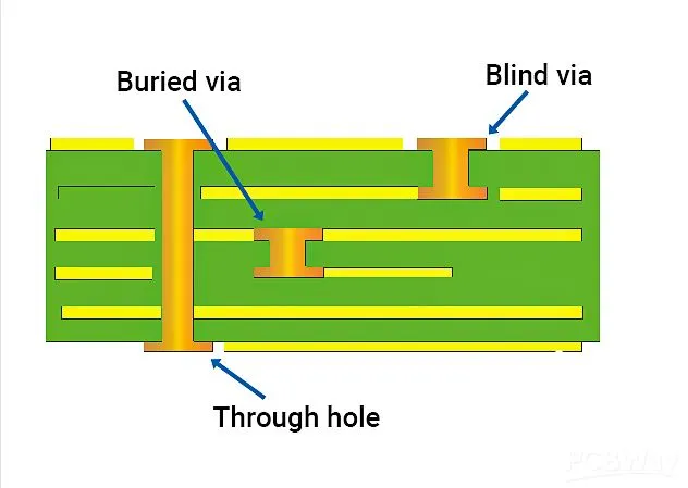
Drilling is one of the most critical and costly steps in PCB manufacturing. It involves creating precise holes for through-hole vias, blind vias, buried vias, and microvias, which enable electrical connections between layers or secure components. Even a minor error in hole placement or quality can lead to signal integrity issues, reduced reliability, or scrapped boards. For instance, a misaligned via in a high-speed PCB can introduce impedance mismatches, causing signal reflections that degrade performance at frequencies above 10 GHz.
Both mechanical and laser drilling aim to achieve high precision, but they differ significantly in their approach, capabilities, and suitability for specific applications. To make an informed decision, let's break down each method's mechanics, benefits, and challenges.
Mechanical Drilling: The Traditional Workhorse
How It Works
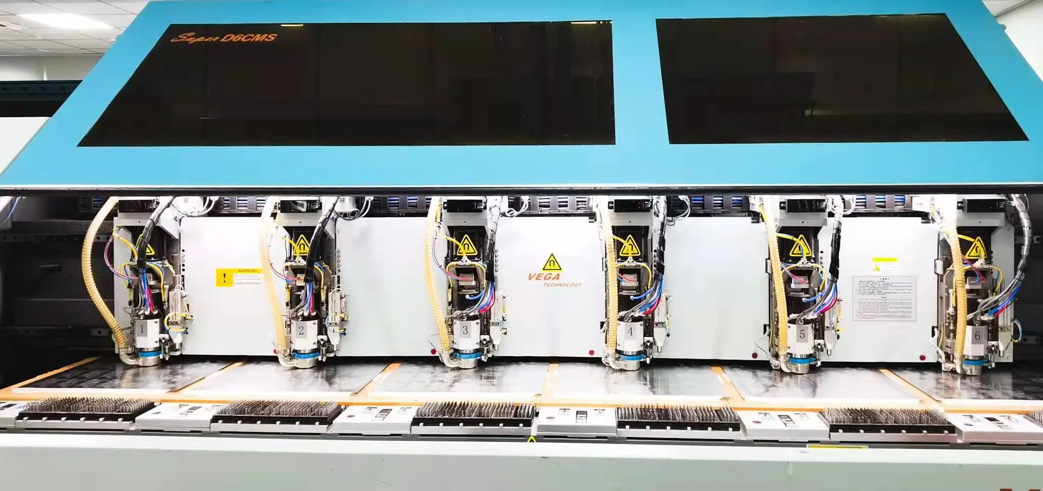
Mechanical drilling uses a rotating drill bit, typically made of micro-grain carbide, to physically remove material from the PCB substrate. These bits, available in sizes as small as 6 mils (0.006 inches), cut through materials like FR4 (fiberglass and resin) or denser substrates like Rogers. The process is controlled by CNC machines, which ensure precise hole placement at speeds up to 300,000 RPM.
Advantages of Mechanical Drilling
1. Depth Control: Mechanical drills offer excellent control over hole depth, making them ideal for blind vias and backdrilling. For example, backdrilling removes excess copper from via stubs to reduce signal reflections in high-speed designs, maintaining signal integrity at 25 Gbps or higher.
2. Consistency: The rotating bit produces uniform, high-quality holes with minimal tapering, ensuring reliable copper plating for vias. This consistency is crucial for thick boards (e.g., 3.2 mm) with aspect ratios up to 10:1.
3. Cost-Effectiveness for Larger Holes: For holes larger than 0.15 mm, mechanical drilling is often more economical due to lower equipment costs and faster throughput compared to laser systems.
4. Versatility: Mechanical drills handle a wide range of substrates, from standard FR4 to high-frequency materials like PTFE, without requiring specialized material properties.
Limitations of Mechanical Drilling
1. Minimum Hole Size: The smallest achievable hole diameter is around 6 mils (0.15 mm), limited by drill bit size and durability. Bits smaller than 8 mils (0.008 inches) are prone to breakage, especially in dense substrates.
2. Debris and Burrs: The physical cutting process generates copper burrs and debris, necessitating additional deburring and desmearing steps. These post-processing tasks increase production time and costs.
3. Wear and Tear: Drill bits wear out after 800 hits on softer materials like FR4 or 200 hits on denser materials like Rogers, leading to potential quality issues if not monitored.
4. Not Ideal for Microvias: For HDI PCBs requiring microvias (holes <0.15 mm), mechanical drilling lacks the precision and speed of laser systems.
Laser Drilling: Precision for the Modern Era
How It Works
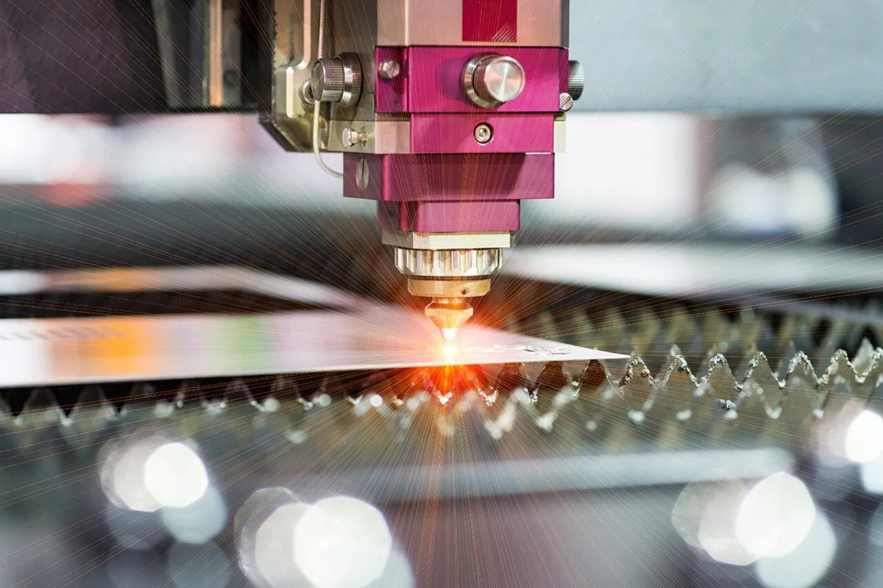
Laser drilling employs a high-energy laser beam (typically CO2 or UV) to vaporize PCB material, creating holes without physical contact. The beam's diameter and exposure time determine the hole size and depth, respectively. Advanced optics focus the beam to achieve holes as small as 1 mil (0.025 mm), ideal for microvias in HDI designs.
Advantages of Laser Drilling
1. Ultra-Small Holes: Laser drilling excels at creating microvias with diameters as small as 50 µm (0.05 mm), critical for HDI PCBs used in smartphones, wearables, and medical devices. For example, a 100 µm microvia enables denser routing in a 0.8 mm pitch BGA package.
2. High Precision and Speed: Lasers offer tight tolerances (±0.01 mm) and can drill thousands of holes per minute, boosting throughput for complex designs with high via counts.
3. Non-Contact Process: The absence of physical contact eliminates mechanical stress, reducing the risk of delamination or microcracking in fragile substrates like polyimide or flexible PCBs.
4. Material Flexibility: Lasers can ablate a wide range of materials, including ceramics, glass, and composites, without requiring specific drill bit sizes.
5. Clean Process: Laser drilling.FactoryImpl produces minimal debris, reducing the need for extensive post-processing like deburring.
Limitations of Laser Drilling
1. Depth Limitations: Lasers struggle with deep holes due to energy loss, typically limited to aspect ratios of 1:1 or less. For instance, a 100 µm microvia can only penetrate about 100 µm deep without a metal stop layer.
2. Tapering and Carbonization: Laser-drilled holes often exhibit tapering (inverted trapezoid shape) and carbonized edges, which can affect plating quality and require additional etching steps.
3. Material Compatibility: Not all laminates are laser-drillable. Prepregs must be specifically designed to avoid excessive ablation or damage to copper layers.
4. Higher Costs: Laser drilling equipment is more expensive, and the process can be slower for larger holes (>0.15 mm), increasing costs for certain applications.
Comparing Key Applications: When to Choose Each Method
Through-Hole Vias
Through-hole vias, which span the entire PCB thickness, are the simplest to manufacture. Both mechanical and laser drilling can handle these, but the choice depends on hole size and board thickness:
- Mechanical Drilling: Preferred for holes ≥0.15 mm and thick boards (e.g., 2.4 mm) due to its depth control and cost-effectiveness.
- Laser Drilling: Suitable for smaller through-holes in thin boards (<0.8 mm), where speed and precision outweigh depth limitations.
Blind and Buried Vias
Blind vias (surface to inner layer) and buried vias (inner layers only) require precise depth control:
- Mechanical Drilling: Excels in backdrilling for blind vias, removing via stubs to minimize deterministic jitter in high-speed signals (e.g., 56 Gbps PAM4).
- Laser Drilling: Ideal for blind microvias in HDI designs, offering smaller diameters and cleaner holes but requiring careful depth management.
Microvias for HDI Designs
Microvias (<0.15 mm) are essential for high-density interconnects:
- Mechanical Drilling: Not viable due to size limitations and slow speeds for small holes.
- Laser Drilling: The go-to method for microvias, enabling high-density routing in compact devices like 5G modules or wearables.
Suggested Reading:Mastering Microvia Formation in HDI Assembly: Laser Drilling Techniques
Flexible and Rigid-Flex PCBs
Flexible PCBs demand minimal mechanical stress:
- Mechanical Drilling: Risky due to potential damage to delicate materials like polyimide.
- Laser Drilling: Preferred for its non-contact nature, ensuring clean holes without compromising flexibility.
Technical Considerations: Aspect Ratio and Pad-to-Hole Ratio
Aspect Ratio
The aspect ratio (hole depth to diameter) impacts manufacturability and reliability:
- Mechanical Drilling: Supports higher aspect ratios (up to 10:1), suitable for thick boards. For example, a 2 mm deep hole can have a 0.2 mm diameter.
- Laser Drilling: Limited to lower aspect ratios (≤1:1) due to depth constraints, requiring thinner dielectric layers for microvias.
High aspect ratios increase plating complexity, risking via cracking or poor copper deposition. Engineers must balance board thickness and via size to avoid these issues.
Pad-to-Hole Ratio
The pad-to-hole ratio ensures sufficient copper for reliable connections:
- Mechanical Drilling: A 0.15 mm via typically requires a 0.3 mm pad (2:1 ratio) to accommodate plating and alignment tolerances.
- Laser Drilling: Microvias (e.g., 0.1 mm) need smaller pads (e.g., 0.25 mm), enabling denser layouts but demanding precise alignment.
For high-speed designs, minimizing pad size reduces parasitic capacitance, improving signal integrity at frequencies above 5 GHz.
Cost and Efficiency: A Practical Perspective
Mechanical Drilling
- Pros: Lower equipment costs and faster drilling for larger holes make it cost-effective for standard PCBs. For example, a 4 layer PCB with 0.3 mm vias can be drilled economically at scale.
- Cons: Additional deburring and desmearing steps, along with bit replacement costs, add to the overall expense.
Laser Drilling
- Pros: High throughput for microvias and reduced post-processing save time in HDI production. A single laser system can drill 10,000 microvias per minute in a 0.4 mm thick board.
- Cons: Higher initial investment and material-specific requirements increase costs, especially for non-HDI designs.
For prototyping, mechanical drilling is often more affordable, while laser drilling shines in mass production of complex, high-density boards.
Choosing the Right Method for Your PCB
The decision between mechanical and laser drilling hinges on your project's requirements:
- Choose Mechanical Drilling for:
- Thicker boards (>1.6 mm) with larger vias (≥0.15 mm).
- Applications requiring deep, high-aspect-ratio holes, like automotive or industrial PCBs.
- Cost-sensitive projects with standard designs.
- Choose Laser Drilling for:
- HDI boards with microvias (<0.15 mm) for compact electronics.
- Flexible or rigid-flex PCBs needing minimal mechanical stress.
- High-volume production where speed and precision are paramount.
For mixed designs, many manufacturers combine both methods, using mechanical drilling for through-holes and laser drilling for microvias. Consulting with your PCB fabricator early in the design phase ensures alignment with their capabilities and minimizes costly revisions.
How ALLPCB Supports Your Drilling Needs
At ALLPCB, we understand that selecting the right drilling method is critical to your PCB's performance and reliability. Our advanced manufacturing facilities are equipped with state-of-the-art mechanical and laser drilling systems, enabling us to handle everything from standard multilayer boards to complex HDI designs. With our quick-turn prototyping, global logistics, and dedicated engineering support, we streamline the fabrication process, ensuring precision and fast delivery.
Conclusion: Making an Informed Choice
Both mechanical and laser drilling play vital roles in PCB manufacturing, each excelling in specific scenarios. Mechanical drilling offers unmatched depth control and cost-effectiveness for standard and thick boards, while laser drilling provides unparalleled precision for microvias and HDI designs. By considering factors like hole size, board thickness, material type, and production volume, engineers can select the method that best aligns with their project's goals.
To optimize your PCB design, collaborate closely with your manufacturer to leverage their drilling capabilities. At ALLPCB, we're committed to empowering engineers with the tools and expertise needed to bring innovative electronics to life. Ready to start your next PCB project? Reach out to us for tailored solutions that meet your unique needs.


