 ALLPCB


If you're diving into the world of printed circuit boards (PCBs), you might have come across the term "4 layers PCB." But what exactly is it, and why is it so popular? A 4-layer PCB is a multilayer board with four conductive layers separated by insulating material, offering a balance of complexity, performance, and cost. It’s widely used in modern electronics for improved signal integrity and compact designs, often incorporating specific layer stack-ups and ground (GND) layers for optimal performance. In this comprehensive guide, we’ll break down everything you need to know about 4-layer PCBs, from stack-up designs to the role of ground layers, ensuring you have actionable insights for your next project.
What Is a 4-Layer PCB?
A 4-layer PCB consists of four distinct layers of conductive material, typically copper, separated by insulating layers known as prepreg or core. These boards are a step up from single or double-layer PCBs, providing more space for routing signals and power while maintaining a compact size. This design is ideal for applications requiring moderate complexity, such as consumer electronics, automotive systems, and industrial controls.
The four layers are usually arranged in a specific order, or "stack-up," to optimize performance. A common configuration includes two outer layers for signal routing and two inner layers dedicated to power and ground planes. This setup helps reduce electromagnetic interference (EMI) and improves signal integrity, making 4-layer PCBs a go-to choice for many engineers.
Why Choose a 4-Layer PCB?
Opting for a 4-layer PCB offers several advantages over simpler designs. Let’s explore the key benefits:
- Improved Signal Integrity: With dedicated ground (GND) layers, a 4-layer PCB minimizes noise and crosstalk between signals, ensuring cleaner and faster data transmission. This is critical for high-speed circuits where signal speeds can reach up to 1 GHz or more.
- Compact Design: More layers mean you can pack complex circuits into a smaller footprint, saving valuable space in devices like smartphones or wearables.
- Better EMI Control: Ground and power planes act as shields, reducing electromagnetic interference, which is essential for meeting regulatory standards.
- Cost-Effective for Medium Complexity: While more expensive than 2-layer boards, 4-layer PCBs strike a balance between cost and performance, avoiding the higher expenses of 6 or 8-layer designs.
For projects that don’t need extreme complexity but still require reliable performance, a 4-layer PCB is often the sweet spot.
Understanding 4-Layer PCB Stack-Up Designs
The term "layer PCB stack-up" refers to the arrangement of conductive and insulating layers in a PCB. For a 4-layer PCB, the stack-up is crucial because it directly impacts signal quality, power distribution, and EMI compliance testing performance. Let’s dive into the most common stack-up configuration and why it works so well.
Standard 4-Layer PCB Stack-Up
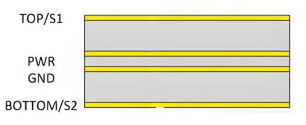
The typical stack-up for a 4-layer PCB is as follows:
- Top Layer (Layer 1): Used for signal routing and component placement. This is where most of your high-speed signals or critical traces are routed.
- Inner Layer 1 (Layer 2): Dedicated as a ground (GND) plane. This layer provides a reference plane for signals on the top layer, reducing noise and ensuring stable return paths.
- Inner Layer 2 (Layer 3): Often used as a power plane to distribute voltage across the board, ensuring consistent power delivery to components.
- Bottom Layer (Layer 4): Another signal layer for additional routing or component placement, with signals referenced to the ground plane above.
This configuration is popular because it sandwiches the signal layers between ground and power planes, creating a controlled impedance environment. For instance, a typical trace impedance on the top layer might be designed to 50 ohms, a standard for many high-speed signals, thanks to the proximity of the ground plane.
Suggested Reading: Optimizing 4-Layer PCB Layer Stackup: A Practical Guide
Alternative Stack-Up Configurations
While the above stack-up is the most common, variations exist depending on project needs:
- Double Ground Planes: Both inner layers (2 and 3) are used as ground planes for maximum EMI shielding, while signals are routed on the top and bottom layers. This is ideal for very noisy environments.
- Signal-Focused Design: In some cases, three layers might be used for signals, with only one inner layer as a ground plane. This sacrifices some noise control for additional routing space.
Choosing the right stack-up depends on your circuit’s requirements, such as signal speed, power needs, and EMI constraints. Always simulate or consult design guidelines to ensure the stack-up meets your impedance and performance goals.
The Role of Ground (GND) Layers in 4-Layer PCBs
Ground (GND) layers are a cornerstone of effective PCB design, especially in a 4-layer setup. But what exactly do they do, and why are they so important? Let’s break it down.
What Are Ground Layers?
A ground layer, often called a GND plane, is a continuous layer of copper connected to the ground of the circuit. In a 4-layer PCB, it’s typically one of the inner layers (Layer 2 in the standard stack-up). This plane serves as a reference point for all signals and provides a low-impedance path for return currents.
Why Ground Layers Matter
Ground layers play several critical roles:
- Noise Reduction: They minimize crosstalk and interference by providing a stable reference for signal traces. Without a proper GND plane, high-speed signals (e.g., running at 500 MHz) can suffer from jitter or data loss.
- Return Path for Currents: Every signal needs a return path back to its source. A dedicated GND layer ensures this path is short and direct, reducing loop inductance and improving performance.
- EMI Shielding: A ground plane acts as a barrier, absorbing stray electromagnetic fields and preventing them from interfering with nearby traces or external devices.
In a 4-layer PCB, placing the GND layer close to signal layers (typically 0.2 mm or less, depending on dielectric thickness) ensures tight coupling, which is vital for maintaining signal integrity at high frequencies.
Best Practices for Ground Layer Design
To get the most out of your GND layers, follow these tips:
- Keep It Continuous: Avoid splitting the ground plane unless absolutely necessary. Breaks in the plane can disrupt return paths and increase noise.
- Use Vias Wisely: Connect components to the GND layer using vias, ensuring a low-impedance connection. Place vias close to component pins to minimize loop areas.
- Avoid Overlapping Signals: Don’t route high-speed signals over splits or gaps in the ground plane on adjacent layers, as this can cause signal reflection and EMI issues.
A well-designed ground layer can make the difference between a reliable circuit and one plagued by noise and failures.
Key Considerations for Designing a 4-Layer PCB
Designing a 4-layer PCB requires careful planning to ensure performance and manufacturability. Here are some critical factors to keep in mind:
Layer Thickness and Material
The thickness of each layer and the dielectric material between them affect impedance and signal speed. Standard 4-layer PCBs often use PCB material FR-4 with a dielectric constant of about 4.2. Typical layer spacing might be 0.2 mm between signal and ground layers to achieve a 50-ohm impedance for high-speed traces. Work with your manufacturer to select the right materials and thicknesses for your design.
Routing Strategies
Routing on a 4-layer PCB should prioritize short, direct traces to minimize signal delay. Keep high-speed signals on the top layer close to the ground plane, and avoid crossing splits in the GND layer. Use the bottom layer for less critical signals or additional routing space.
Suggested Reading: Beyond the Basics: Advanced Routing Techniques for High-Density 4-Layer PCBs
Power Distribution
Dedicate an inner layer to power distribution to ensure stable voltage across the board. Use decoupling capacitors near power pins of ICs to filter noise, placing them as close as possible (within 1-2 mm) to reduce inductance.
Thermal Management
With more layers, heat dissipation can be a concern. Use thermal vias to transfer heat from components to inner layers or add copper pours on outer layers to spread heat evenly.
Common Applications of 4-Layer PCBs
4-layer PCBs are versatile and used across various industries. Some common applications include:
- Consumer Electronics: Smartphones, tablets, and wearables often use 4-layer PCBs for their compact size and ability to handle moderate complexity.
- Automotive Systems: Control units and sensors in vehicles rely on 4-layer designs for reliable performance in harsh environments.
- Industrial Equipment: Automation systems and machinery use these boards for robust power distribution and signal integrity.
- Medical Devices: Portable diagnostic tools benefit from the compact and noise-resistant nature of 4-layer PCBs.
If your project falls into one of these categories, a 4-layer PCB might be the perfect fit.
Challenges and Limitations of 4-Layer PCBs
While 4-layer PCBs offer many benefits, they’re not without challenges:
- Higher Cost: Compared to 2-layer boards, the manufacturing process for 4-layer PCBs is more complex, increasing costs by 30-50% depending on volume and specifications.
- Design Complexity: Routing and layer stack-up require more planning and simulation to avoid signal integrity issues.
- Limited for High Complexity: For extremely dense or high-speed designs (e.g., above 5 GHz), you might need 6 or more layers for adequate routing and shielding.
Understanding these limitations helps you decide if a 4-layer PCB is the right choice or if a different layer count would better suit your needs.
How to Manufacture a 4-Layer PCB
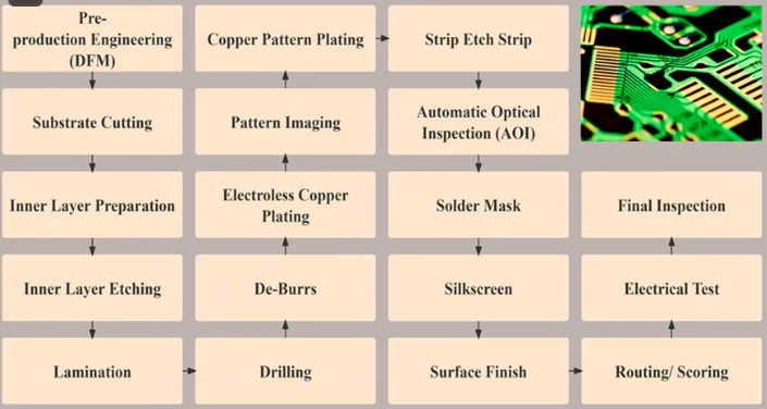
Manufacturing a 4-layer PCB involves several steps, from design to final assembly. Here’s a simplified overview:
- Design Phase: Use PCB design software to create your schematic and layout, defining the layer stack-up and routing.
- Material Selection: Choose the core and prepreg materials, typically FR-4 for standard designs, with specific dielectric thicknesses.
- Lamination: Layers are stacked and bonded together under heat and pressure to form a single board.
- Drilling and Plating: Holes are drilled for vias, and copper is plated to connect layers.
- Etching and Finishing: Unwanted copper is removed, and a protective finish (like ENIG or HASL) is applied to the board.
Partnering with a reliable PCB manufacturer ensures that your design is translated into a high-quality board with precise layer alignment and impedance control.
Final Thoughts on 4-Layer PCBs
A 4-layer PCB is a powerful tool for engineers looking to balance performance, cost, and complexity in their designs. With a well-planned layer PCB stack-up and properly designed ground (GND) layers, you can achieve excellent signal integrity, reduced EMI, and compact layouts suitable for a wide range of applications. Whether you’re working on consumer electronics, automotive systems, or industrial equipment, understanding the nuances of 4-layer PCB design can elevate your projects to the next level.
By focusing on critical aspects like stack-up configuration, ground plane design, and routing strategies, you can avoid common pitfalls and ensure a reliable, high-performing board. Keep these insights in mind as you plan your next PCB design, and you’ll be well-equipped to tackle the challenges of modern electronics.


