ALLPCB


In the fast-paced world of modern electronics, high-speed printed circuit board (PCB) designs are critical for ensuring reliable data transmission in applications like USB, HDMI, Ethernet, and PCIe. At the heart of these designs lies differential pair routing, a technique that enhances signal integrity, minimizes noise, and supports high-speed communication. For engineers, mastering differential pair routing is essential to creating robust and efficient PCBs that meet stringent performance requirements.
In this blog, we dive deep into the principles, techniques, and best practices for differential pair routing in high-speed PCB layouts. Whether you're designing a compact IoT device or a complex data center system, these insights will help you optimize your designs for signal integrity and performance.
What Are Differential Pairs and Why Do They Matter?
Differential pairs consist of two traces that carry equal and opposite signals, typically referenced to a common ground plane. Unlike single-ended signaling, where a single trace relies on a ground plane for the return path, differential signaling uses the voltage difference between the two traces to transmit data. This approach offers several advantages:
-
Noise Immunity: Common-mode noise, such as electromagnetic interference (EMI), affects both traces equally and is canceled out at the receiver.
-
Signal Integrity: Differential pairs maintain signal quality over longer distances, making them ideal for high-speed interfaces.
-
Higher Data Rates: Protocols like USB (90 ohms impedance) and PCIe (85 ohms) leverage differential pairs for reliable, high-speed communication.
Differential pairs are standard in high-speed interfaces, including USB 3.0 (5 Gbps), HDMI 2.0 (6 Gbps per channel), and Ethernet (10 Gbps). However, their benefits come with strict routing requirements to maintain symmetry, impedance, and signal timing.
Recommended Reading: Impedance Control: How to Achieve Precision in High-Speed PCB Designs
Key Principles of Differential Pair Routing
To achieve optimal performance, differential pair routing must adhere to several fundamental principles. These ensure that the signals remain synchronized, impedance is controlled, and noise is minimized.
1. Maintain Trace Symmetry
Symmetry between the two traces is critical. Both traces must have identical lengths, widths, and spacing to ensure that the signals arrive at the receiver simultaneously. Any mismatch can introduce skew, leading to timing errors. For example, a 1 mm length mismatch in a 10 Gbps signal can cause a delay of approximately 6.7 ps, potentially violating timing margins.
2. Control Impedance
Differential pairs require a specific differential impedance, typically defined by the signaling standard (e.g., 90 ohms for USB, 100 ohms for Ethernet). Impedance is influenced by trace width, spacing, and the dielectric properties of the PCB material. Maintaining consistent impedance along the entire trace length prevents signal reflections and degradation.
3. Minimize Crosstalk
Crosstalk occurs when signals from adjacent traces interfere with the differential pair. To reduce crosstalk, maintain a clearance of at least three times the trace width between differential pairs and other traces. For high-speed signals, consider broadside routing on adjacent layers to increase routing density while controlling crosstalk.
4. Optimize Return Paths
A solid ground plane beneath the differential pair provides a low-impedance return path, reducing EMI and ensuring signal integrity. Avoid routing differential pairs over split planes, as this disrupts the return path and creates a loop antenna effect, increasing noise.
Best Practices for Differential Pair Routing
Based on industry standards and insights from high-performing PCB design resources, here are actionable best practices to guide your differential pair routing.
1. Route Traces Together
Keep the two traces of a differential pair as close as possible throughout their path. Tight coupling (e.g., spacing of 5-10 mils for a 5-mil trace width) ensures that both traces experience similar electrical conditions, reducing noise and distortion. Use PCB design tools like Cadence or Altium to define differential pair constraints, ensuring consistent spacing and width.
2. Match Trace Lengths
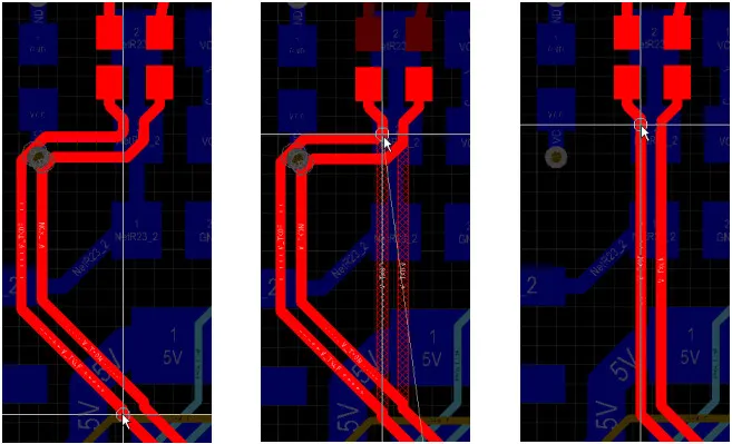
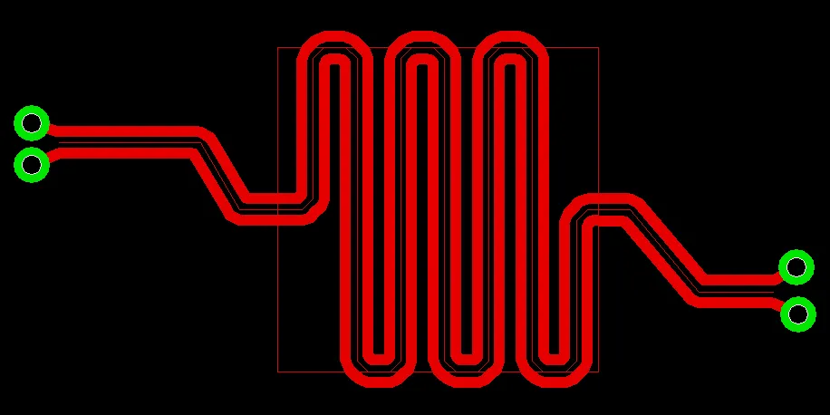
Length matching is critical to avoid skew. For high-speed interfaces like PCIe, the length tolerance is typically ±5 mils within a pair. Use serpentine routing (also called trombone routing) to extend the shorter trace, but design the geometry carefully to minimize impedance discontinuities. For example, keep serpentine bends smooth with 135° angles to reduce EMI.
3. Minimize Vias
Vias introduce impedance discontinuities and signal degradation. If vias are unavoidable, place them symmetrically for both traces and use the same number of vias per trace. For example, in a 4-layer PCB, transitioning a differential pair from the top layer to an inner layer requires two vias (one per trace), placed equidistant from the pads. Consider back-drilling vias to shorten stub lengths and reduce reflections.
4. Route on the Same Layer
Routing both traces on the same layer ensures consistent impedance and signal speed. Signal propagation varies between layers due to differences in dielectric constants (e.g., FR-4 has a dielectric constant of ~4.2). If layer transitions are necessary, use stitching capacitors to maintain a continuous return path across reference planes.
5. Use a Solid Ground Plane
A continuous ground plane beneath the differential pair minimizes EMI and provides a stable reference. For a 4-layer PCB, dedicate one inner layer to a full ground plane. Avoid routing traces over split planes, as this disrupts the return path and increases noise coupling. If a split plane is unavoidable, route the traces around it or use stitching capacitors.
6. Place Coupling Capacitors Symmetrically
Some high-speed differential pairs, such as those in PCIe, require serial coupling capacitors. Use smaller packages (e.g., 0402 instead of 0603) to minimize impedance discontinuities, and place capacitors symmetrically to maintain signal timing. For example, a 0.1 µF capacitor placed 50 mils from the transmitter ensures balanced signal propagation.
Common Challenges and Solutions
Differential pair routing presents several challenges, particularly in high-density or high-speed designs. Here are common issues and how to address them:
1. Crosstalk from Adjacent Traces
Challenge: Nearby single-ended traces or other differential pairs can induce crosstalk, degrading signal quality.
Solution: Increase spacing to at least 3x the trace width (e.g., 15 mils for a 5-mil trace). Use guard traces grounded with vias at regular intervals (e.g., every 500 mils) to shield sensitive pairs.
2. Impedance Mismatches
Challenge: Variations in trace width, spacing, or dielectric thickness can cause impedance mismatches, leading to reflections.
Solution: Use a field solver in your PCB design tool to calculate trace geometry for the target impedance (e.g., 100 ohms for Ethernet). Verify the stackup with your manufacturer to ensure consistent dielectric properties.
3. Skew from Asymmetric Routing
Challenge: Asymmetric routing around components or vias can introduce skew, disrupting signal timing.
Solution: Use symmetric fan-out patterns at the driver and receiver ends. For example, when routing from a fine-pitch BGA, ensure equal track lengths to the fan-out vias, as recommended by Zuken's design guidelines.
4. Manufacturing Constraints
Challenge: Tight trace spacing or small via sizes may exceed manufacturing capabilities, increasing costs or defects.
Solution: Consult your PCB manufacturer early to confirm minimum trace width (e.g., 4 mils) and spacing (e.g., 4 mils). Adjust your design rules to balance performance and manufacturability.
Advanced Techniques for High-Speed Designs
For cutting-edge applications, such as 5G or data center equipment, consider these advanced techniques:
1. Broadside Differential Pairs
Route differential pairs on adjacent signal layers (broadside configuration) to increase routing density and reduce crosstalk. This requires precise stackup design to maintain impedance, as the dielectric thickness between layers affects coupling.
2. Zigzag Routing
To mitigate fiber weave effects in high-speed designs, route traces at a 15° angle on alternating layers. This reduces crosstalk and improves signal integrity, especially for dual stripline configurations.
Recommended Reading: PCB Lamination for High-Speed Designs: Techniques and Considerations
3. Signal Integrity Simulation
Before fabrication, use simulation tools like Altium Designer's signal integrity analyzer to predict differential pair behavior. Simulate impedance, crosstalk, and propagation delay to identify issues early, saving time and costs.
How ALLPCB Supports High-Speed PCB Design
At ALLPCB, we understand the complexities of high-speed PCB design and differential pair routing. Our advanced manufacturing capabilities and quick-turn prototyping services empower engineers to bring their designs to life with confidence. With global logistics and state-of-the-art facilities, we ensure precise fabrication of high-speed PCBs, meeting tight tolerances for trace width, spacing, and impedance control. Whether you're prototyping a 5G module or scaling production for IoT devices, ALLPCB's expertise and rapid delivery help you achieve reliable, high-performance results.
Conclusion
Differential pair routing is a cornerstone of high-speed PCB design, enabling robust signal transmission in today's advanced electronics. By adhering to principles like trace symmetry, impedance control, and proper return paths, engineers can minimize noise and ensure signal integrity. Best practices, such as length matching, minimal via usage, and solid ground planes, further enhance performance, while advanced techniques like broadside routing and signal simulation address the demands of cutting-edge applications.
By applying these techniques and leveraging modern PCB design tools, you can create layouts that meet the stringent requirements of high-speed interfaces. At ALLPCB, we're committed to supporting your journey with high-quality manufacturing and prototyping services tailored to your needs.