 ALLPCB


In the world of printed circuit board (PCB) design, achieving optimal signal integrity is crucial for high-speed and high-frequency applications. Two key factors that significantly impact performance are PCB impedance control and material selection. But how do these elements work together to ensure reliable signal transmission? In short, impedance control ensures that signals travel without distortion by matching the electrical characteristics of traces, while the right material selection supports this by providing the necessary dielectric properties and stability for high-frequency signals.
This blog post dives deep into the intricacies of PCB material selection for impedance, how to optimize PCB material for signal integrity, and the essentials of PCB impedance analysis. Whether you're an engineer working on high-speed designs or a designer looking to enhance performance, this comprehensive guide will provide actionable insights and practical tips to elevate your PCB projects.
Understanding PCB Impedance Control: The Foundation of Signal Integrity
Impedance control in PCB design refers to the process of designing traces and layouts to maintain a specific electrical impedance, ensuring that signals travel through the board without reflections or distortions. In high-speed circuits, such as those used in telecommunications or data processing, even a slight mismatch in impedance can lead to signal loss, crosstalk, or electromagnetic interference (EMI).
Impedance is measured in ohms and typically ranges between 50 to 100 ohms for most high-speed designs, depending on the application. For example, USB 2.0 signals often require a differential impedance of 90 ohms, while Ethernet applications might target 100 ohms. Achieving these precise values requires careful design of trace width, spacing, and the dielectric environment surrounding the traces.
Why is impedance control important? Without it, signal integrity suffers. Reflections caused by impedance mismatches can degrade data transmission, leading to errors or reduced performance. By controlling impedance, designers can ensure that signals arrive at their destination with minimal distortion, preserving the integrity of the data being transmitted.
The Role of PCB Material Selection in Impedance Control
When it comes to PCB material selection for impedance, the choice of substrate and dielectric materials plays a pivotal role. The dielectric constant (Dk) and loss tangent (Df) of a material directly affect how signals propagate through the board. Let’s break this down:
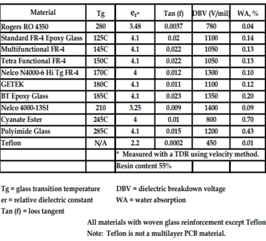
- Dielectric Constant (Dk): This value determines the speed at which signals travel through the material. A lower Dk allows for faster signal propagation, which is critical for high-frequency designs. For instance, standard FR-4 materials have a Dk of around 4.2-4.5, while high-frequency materials like Rogers RO4350B offer a Dk of approximately 3.48, making them better suited for RF applications.
- Loss Tangent (Df): This measures the signal loss due to the material. A lower Df means less energy is lost as heat, which is essential for maintaining signal strength over long traces. High-frequency materials often have a Df as low as 0.003, compared to FR-4’s typical 0.02.
Selecting the right material involves balancing performance with cost. While advanced laminates offer superior electrical properties, they are often more expensive. For budget-conscious projects, standard FR-4 might suffice for lower-frequency applications, but for high-speed designs operating above 1 GHz, specialized materials become necessary to optimize PCB material for signal integrity.
Factors Influencing PCB Impedance Analysis
Conducting a thorough PCB impedance analysis is essential to ensure that your design meets the required specifications. Several factors influence impedance, and understanding these can help you fine-tune your PCB layout for optimal performance. Here are the key elements to consider:
1. Trace Geometry
The width, thickness, and spacing of traces directly impact impedance. Wider traces generally have lower impedance, while narrower traces increase it. For example, a 50-ohm single-ended trace on a standard FR-4 board might require a width of about 6 mils (0.006 inches) with a specific stack-up. Tools like impedance calculators can help determine the exact dimensions based on your material and layer configuration.
2. Stack-Up Design
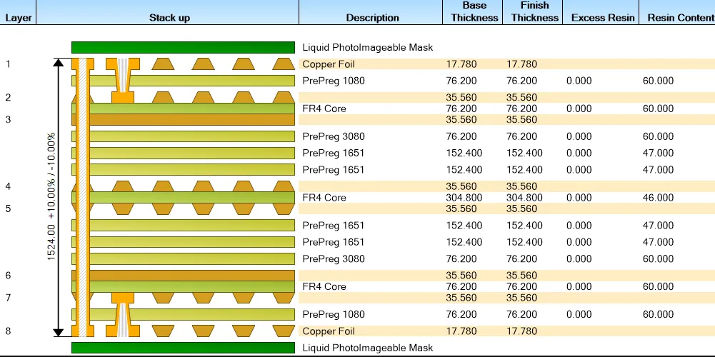
The arrangement of copper layers and dielectric materials in a PCB stack-up affects impedance. A typical 4-layer board might have signal layers on the top and bottom with ground and power planes in the middle. Maintaining consistent spacing between signal traces and reference planes is crucial for controlled impedance. Variations in dielectric thickness can lead to impedance deviations, so precision in manufacturing is key.
3. Frequency of Operation
Signal frequency influences how impedance behaves. At higher frequencies, skin effect and dielectric losses become more pronounced, requiring materials with lower Dk and Df values. For instance, a design operating at 5 GHz will have stricter material and impedance requirements compared to one at 100 MHz.
How to Optimize PCB Material for Signal Integrity
To optimize PCB material for signal integrity, designers must consider both the electrical and mechanical properties of the materials they choose. Here are actionable steps to guide your material selection process:
- Define Your Frequency Requirements: Determine the operating frequency of your design. For applications below 1 GHz, standard FR-4 might work well. For higher frequencies, consider low-loss laminates designed for RF and microwave applications.
- Evaluate Thermal Performance: High-frequency designs often generate more heat. Materials with good thermal conductivity can help dissipate heat and maintain signal integrity over time.
- Consider Manufacturing Constraints: Some advanced materials require specialized fabrication processes, which can increase costs and lead times. Ensure that your chosen material aligns with your production capabilities.
- Test and Simulate: Use simulation tools to model how different materials affect impedance and signal integrity. Software can predict signal behavior and help you choose the best material before fabrication.
By following these steps, you can ensure that your material choice supports both impedance control and overall performance, minimizing signal loss and interference.
Practical Tips for Implementing Impedance Control in PCB Design
Beyond material selection, there are several design practices that can help maintain controlled impedance and enhance signal integrity. These tips are practical and can be applied to most high-speed PCB projects:
- Use Reference Planes: Place ground or power planes adjacent to signal layers to provide a consistent return path for signals. This helps stabilize impedance and reduces EMI.
- Minimize Via Usage: Vias can introduce impedance discontinuities. When unavoidable, use back-drilling or buried vias to reduce their impact on signal integrity.
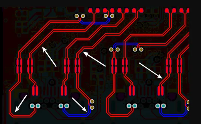
- Route Traces Carefully: Avoid sharp bends in traces, as they can cause signal reflections. Use 45-degree angles or curved traces for smoother transitions.
- Match Trace Lengths: For differential pairs, ensure that both traces are of equal length to prevent timing skew and maintain impedance balance.
Implementing these strategies during the design phase can significantly improve the performance of your PCB, especially in high-speed applications.
Common Challenges in PCB Impedance Control and How to Overcome Them
Even with careful planning, challenges can arise during the design and manufacturing of PCBs with controlled impedance. Here are some common issues and solutions:
1. Manufacturing Tolerances
Variations in trace width or dielectric thickness during fabrication can lead to impedance deviations. To mitigate this, work closely with your manufacturer to define tight tolerances (e.g., ±10% for impedance) and request test coupons to verify impedance after production.
2. Material Inconsistencies
Not all batches of PCB materials have identical properties. Request material datasheets and ensure that your supplier provides consistent quality. If possible, stick to well-known material families with proven performance.
3. High-Frequency Signal Loss
At very high frequencies, signal loss due to dielectric absorption becomes a concern. Choosing a material with a low loss tangent and optimizing trace lengths can help reduce this effect.
Addressing these challenges upfront can save time and resources, ensuring that your design performs as intended in real-world applications.
Conclusion: Balancing Impedance Control and Material Selection for Optimal PCB Performance
In summary, PCB impedance control and material selection are two sides of the same coin when it comes to achieving excellent signal integrity. By understanding the principles of PCB impedance analysis, carefully selecting materials to optimize PCB material for signal integrity, and applying best practices in design, you can create high-performing circuit boards that meet the demands of modern electronics.
Whether you're designing for high-speed data transmission or RF applications, the insights provided in this guide can help you navigate the complexities of PCB material selection for impedance. With the right approach, you can minimize signal distortions, reduce EMI, and ensure reliable performance in even the most challenging environments.
At ALLPCB, we are committed to supporting your design journey with high-quality manufacturing solutions tailored to your needs. By leveraging the strategies outlined in this blog, you can take your PCB designs to the next level and achieve outstanding results.


