 ALLPCB


In the world of High-Density Interconnect (HDI) PCB design, maximizing component density is a top priority for engineers looking to create compact, high-performance electronics. One powerful technique to achieve this is via-in-pad technology. This approach allows designers to place vias directly under component pads, saving valuable board space and improving signal integrity. If you're searching for ways to optimize your HDI PCB layout, via-in-pad offers significant advantages, provided you follow specific design rules and component placement strategies.
In this comprehensive guide, we'll dive deep into the benefits of via-in-pad in HDI PCB design, outline essential design rules, and share best practices for component placement. Whether you're an experienced engineer or new to HDI technology, this blog will provide actionable insights to enhance your designs. Let's explore how via-in-pad can transform your PCB projects.
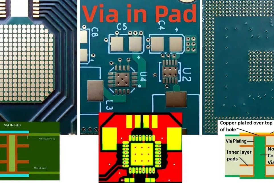
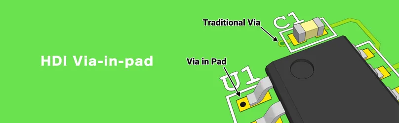
What is Via-in-Pad in HDI PCB Design?
Via-in-pad refers to a design technique where vias—small holes that connect different layers of a PCB—are placed directly beneath the pads of surface-mount components. Unlike traditional vias, which are positioned away from component pads and require additional routing space, via-in-pad integrates the via into the pad itself. This is especially useful in HDI PCB design, where space is limited, and wiring density is high.
In HDI boards, which are defined by their fine lines, small vias, and high component density, via-in-pad technology helps reduce the overall footprint of the PCB. By eliminating the need for extra space around components for vias, designers can pack more components into a smaller area. This technique is commonly used in applications like smartphones, wearables, and medical devices, where miniaturization is critical.
HDI PCB Via-in-Pad Advantages
Using via-in-pad in HDI PCB design comes with several benefits that directly impact performance, space efficiency, and manufacturing. Here are the key advantages:
1. Increased Component Density
The primary benefit of via-in-pad is the ability to place components closer together. Traditional via placement requires breakout traces and additional space, which can limit how many components fit on a board. With via-in-pad, you can reduce the spacing between components, achieving up to 20-30% higher density in some designs. This is crucial for compact devices where every millimeter counts.
2. Improved Signal Integrity
Placing vias directly under pads shortens the signal path, reducing inductance and resistance. For high-speed designs, this can lower signal delay and improve performance. For example, in a design operating at 5 GHz, via-in-pad can help maintain signal integrity by minimizing parasitic effects, ensuring cleaner data transmission compared to longer trace routes.
3. Reduced Board Size
By eliminating the need for separate via placement areas, via-in-pad allows for smaller overall PCB dimensions. This not only cuts down on material costs but also meets the demand for miniaturization in modern electronics. A smaller board can also mean lighter devices, which is a key factor in industries like aerospace and wearables.
4. Enhanced Thermal Management
Vias under pads can act as thermal pathways, helping to dissipate heat from components like power ICs. In designs with high-power components, via-in-pad can reduce thermal resistance by up to 15%, ensuring better heat distribution across layers and preventing overheating issues.
5. Simplified Routing
With vias integrated into pads, routing becomes less complex. Designers no longer need to route traces around external vias, which can reduce the number of layers required in some HDI designs. This simplification can lower manufacturing costs and improve design turnaround time.
Via-in-Pad Design Rules for HDI PCB
While via-in-pad offers significant benefits, it requires careful planning to ensure manufacturability and reliability. Following specific design rules is essential to avoid issues like soldering defects or structural weaknesses. Below are the critical guidelines for implementing via-in-pad in HDI PCB design.
1. Via Size and Aspect Ratio
In HDI designs, vias are typically microvias with diameters ranging from 0.1 mm to 0.3 mm. When placing a via in a pad, ensure the via diameter is small enough to fit within the pad without compromising the solder joint. A common rule is to keep the via diameter less than 50% of the pad width. Additionally, maintain an aspect ratio (via depth to diameter) of no more than 0.8:1 to ensure reliable plating during manufacturing.
2. Pad Size and Clearance
The pad must be large enough to accommodate both the via and the solder joint. A general guideline is to increase the pad size by at least 0.2 mm beyond the via diameter to provide sufficient area for soldering. Also, ensure proper clearance between adjacent pads to prevent solder bridging, typically a minimum of 0.15 mm for fine-pitch components.
3. Via Fill and Capping
To prevent solder wicking into the via during assembly, vias in pads must be filled or capped. Conductive epoxy or copper filling is often used, followed by a planarization process to create a flat surface for soldering. Non-conductive filling can also be an option for thermal vias. Ensure the filling material can withstand reflow temperatures, typically up to 260°C, to avoid defects.
4. Layer Stackup Considerations
In HDI PCBs, via-in-pad is often used with blind or buried vias to connect inner layers without affecting outer layer space. When designing the stackup, limit via-in-pad to the top or bottom layers for surface-mount components. Avoid placing via-in-pad on inner layers unless necessary, as this can complicate manufacturing and increase costs by up to 15-20%.
5. Manufacturing Tolerances
Work closely with your PCB fabricator to understand their capabilities for via-in-pad processes. Some manufacturers may have limitations on via drilling precision or filling techniques. Typical tolerances for via placement in pads are ±0.05 mm, so ensure your design accounts for these variations to avoid misalignment during assembly.
HDI PCB Component Placement Techniques with Via-in-Pad
Effective component placement is critical in HDI PCB design, especially when using via-in-pad technology. Poor placement can negate the benefits of via-in-pad and lead to signal issues or assembly challenges. Here are proven techniques to optimize component placement in HDI designs.
1. Prioritize High-Pin-Count Components
Components like BGAs (Ball Grid Arrays) and QFNs (Quad Flat No-leads) with high pin counts benefit most from via-in-pad. Place these components first, using via-in-pad to route signals directly beneath their pads. This minimizes trace length and reduces the need for fan-out routing. For a BGA with a 0.5 mm pitch, via-in-pad can save up to 40% of the routing space compared to traditional methods.
2. Group Related Components
Place components that interact frequently, such as a microcontroller and its supporting capacitors, close together. Using via-in-pad allows you to keep these components compact without sacrificing signal quality. Ensure bypass capacitors are within 1-2 mm of power pins to minimize noise, leveraging via-in-pad for direct connections to power planes.
3. Optimize for Signal Flow
Arrange components to create a logical signal flow, reducing the need for long traces. With via-in-pad, you can route critical signals through inner layers directly under components, maintaining signal integrity. For high-speed signals above 1 GHz, keep trace lengths under 10 mm if possible, using via-in-pad to avoid unnecessary detours.
4. Balance Thermal Distribution
Distribute heat-generating components evenly across the board to prevent hot spots. Use via-in-pad to create thermal vias under power components, connecting them to internal ground planes for heat dissipation. For a power IC dissipating 2 W, placing 4-6 thermal vias under the pad can reduce junction temperature by 10-15°C.
5. Consider Assembly Constraints
Ensure component placement allows for automated assembly processes like pick-and-place machines. Avoid placing small components too close to large ones, as this can cause shadowing during soldering. Maintain a minimum spacing of 0.3 mm between components, even with via-in-pad, to ensure reliable reflow soldering.
Challenges and Solutions for Via-in-Pad in HDI PCB Design
While via-in-pad offers many benefits, it also presents challenges that designers must address. Here are common issues and practical solutions:
Challenge 1: Solder Wicking
If vias are not properly filled, solder can flow into them during assembly, leading to weak joints. Solution: Always specify via filling in your design files and verify with your manufacturer that the process meets industry standards like IPC-4761 for via protection.
Challenge 2: Increased Manufacturing Cost
Via-in-pad often requires advanced fabrication techniques, which can raise costs by 10-20%. Solution: Use via-in-pad selectively for critical components like BGAs, while using traditional vias for less space-constrained areas to balance cost and performance.
Challenge 3: Design Complexity
Integrating vias into pads adds complexity to the design process, especially for multilayer HDI boards. Solution: Leverage advanced PCB design software with built-in via-in-pad support and design rule checks to streamline the process and avoid errors.
Conclusion: Unlocking the Potential of Via-in-Pad in HDI PCB Design
Via-in-pad technology is a game-changer for HDI PCB design, offering a powerful way to maximize component density, improve signal integrity, and reduce board size. By understanding the advantages of via-in-pad, adhering to essential design rules, and applying strategic component placement techniques, engineers can create compact, high-performance designs that meet the demands of modern electronics.
At ALLPCB, we’re committed to supporting your HDI PCB projects with cutting-edge manufacturing solutions tailored to advanced techniques like via-in-pad. Whether you're designing for consumer electronics, medical devices, or industrial applications, incorporating via-in-pad into your workflow can elevate your designs to the next level. Start optimizing your HDI PCB layouts today and experience the difference that via-in-pad can make.


