 ALLPCB


If you're looking for a clear understanding of PCB outline and mounting holes, you're in the right place. This guide answers your core needs: PCB mounting holes are openings drilled into a printed circuit board to secure it to a chassis or enclosure, while the PCB outline defines the board's shape and dimensions. Proper hole placement and outline design are critical for mechanical stability, ease of assembly, and ensuring your board fits perfectly in its intended application. In this comprehensive blog, we'll dive deep into the essentials of PCB outline design, mounting hole types, placement strategies, hardware choices, and best practices to help you create reliable and efficient PCB designs.
Introduction to PCB Outline and Mounting Holes
Designing a printed circuit board (PCB) is more than just placing components and routing traces. Two often-overlooked but vital aspects are the PCB outline and mounting holes. The outline determines the physical shape and size of your board, ensuring it fits within the intended device or enclosure. Mounting holes, on the other hand, provide a way to securely attach the PCB to its housing, preventing movement and ensuring stability during operation. Together, these elements play a crucial role in the functionality and durability of your electronic product.
In this definitive guide, we'll break down everything you need to know about PCB outlines and mounting holes. Whether you're an electronics engineer, a hobbyist, or a product designer, you'll find practical tips and detailed insights to optimize your PCB designs for both performance and manufacturability. We'll cover design considerations, hole placement strategies, types of mounting hardware, and common pitfalls to avoid. Let's get started with the basics.
What Are PCB Outlines and Why Do They Matter?
The PCB outline is the boundary or shape of the board, defining its physical dimensions. It is typically created in the design software as a closed shape on a specific layer, often called the "board outline" or "mechanical layer." This outline tells manufacturers the exact size and form of the PCB, ensuring it fits into the intended enclosure or device casing.
A well-designed outline is essential for several reasons:
- Fit and Compatibility: The outline ensures the PCB fits perfectly within the product's housing, avoiding issues like overlapping components or misalignment.
- Manufacturing Precision: Manufacturers use the outline to cut the board from a larger panel, so accuracy is critical to avoid wasted material or defective boards.
- Mechanical Constraints: The shape can impact how the board interacts with other parts of the device, such as connectors or cooling systems.
When designing the outline, consider the space constraints of your application. For example, a rectangular outline is common for standard enclosures, while irregular shapes may be needed for custom designs like wearable devices. Additionally, ensure the outline accounts for edge clearance—typically 0.5 mm to 1 mm from components or traces—to prevent damage during cutting or handling.
Related Reading: PCB Outline Design Rules: Ensuring Manufacturability and Compatibility
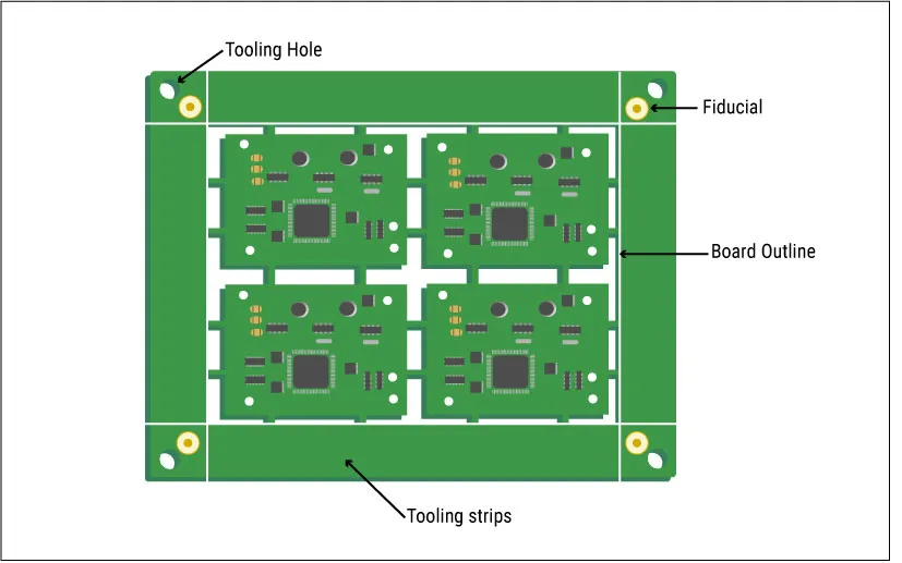
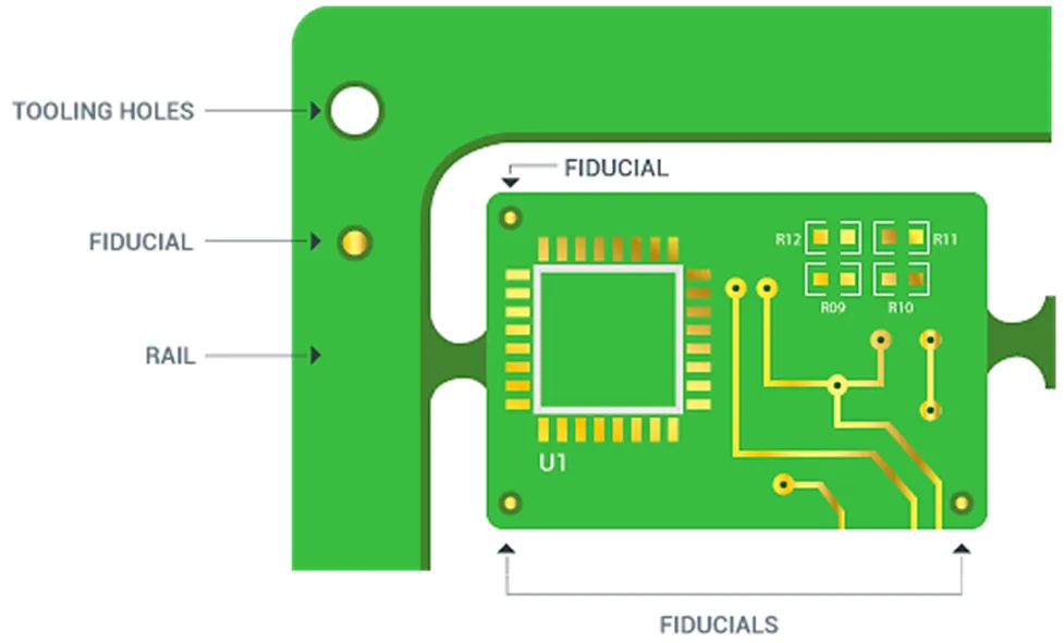
Understanding PCB Mounting Holes
PCB mounting holes are openings drilled through the board to allow it to be fastened to a chassis, enclosure, or another surface. These holes are typically larger than vias or component holes, ranging from 2.5 mm to 5 mm in diameter, depending on the screw or fastener size. They are strategically placed to provide mechanical support and prevent the board from shifting during use, especially in environments with vibration or mechanical stress.
Mounting holes serve multiple purposes beyond just securing the board:
- Grounding: Some mounting holes are plated and connected to the ground plane, helping to reduce electromagnetic interference (EMI).
- Thermal Management: In high-power applications, mounting holes near heat sinks can aid in heat dissipation.
- Alignment: They can double as alignment points during assembly, ensuring components or connectors are positioned correctly.
Types of PCB Mounting Holes
Not all mounting holes are the same. Depending on your design needs, you can choose from several types, each with specific applications and benefits.
1. Plated Through-Holes (PTH)
Plated mounting holes have a conductive layer inside the hole, often connected to the ground plane. These are ideal for applications where grounding or EMI shielding is a priority. For instance, in a high-frequency circuit operating at 2.4 GHz, a plated hole can help maintain signal integrity by reducing noise.
Related Reading: Plated Through-Hole vs. Via: Understanding the Key Differences for PCB Design
2. Non-Plated Through-Holes (NPTH)
Non-plated holes lack a conductive coating and are used purely for mechanical fastening. They are simpler and cheaper to manufacture, making them suitable for low-cost designs where electrical connectivity isn't needed at the mounting point.
3. Countersunk Holes
These holes have a conical shape at the top, allowing flat-head screws to sit flush with the PCB surface. They are useful in designs where a smooth surface is required, such as in consumer electronics with tight enclosures.
4. Tooling Holes
Tooling holes are small, non-plated holes used during manufacturing for alignment on assembly machines. Typically 1 mm to 1.5 mm in diameter, they are placed outside the active area of the board and don't interfere with the final product assembly.
Best Practices for PCB Hole Placement
Proper PCB hole placement is critical to ensure mechanical stability and avoid interference with other board elements. Here are some key guidelines to follow when positioning mounting holes in your design:
- Corner Placement: Place mounting holes at the corners of the PCB to provide balanced support. For a standard rectangular board of 100 mm x 50 mm, position holes 5 mm from each edge to maintain structural integrity.
- Clearance from Components: Maintain a minimum clearance of 3 mm to 5 mm between mounting holes and nearby components or traces to prevent stress or damage during assembly.
- Symmetry: Distribute holes symmetrically to avoid uneven stress on the board, which could lead to warping or cracking under mechanical load.
- Enclosure Alignment: Ensure holes align with the mounting points in the enclosure. Use the enclosure's design files or a 3D model to verify alignment during the PCB design phase.
- Avoid High-Density Areas: Keep holes away from densely populated areas with critical components or high-speed traces (e.g., signals above 100 MHz) to minimize interference.
Choosing the Right PCB Mounting Hardware
Selecting the appropriate mounting hardware is just as important as designing the holes themselves. The hardware must match the hole size, board thickness, and application requirements. Here are some common options and their uses:
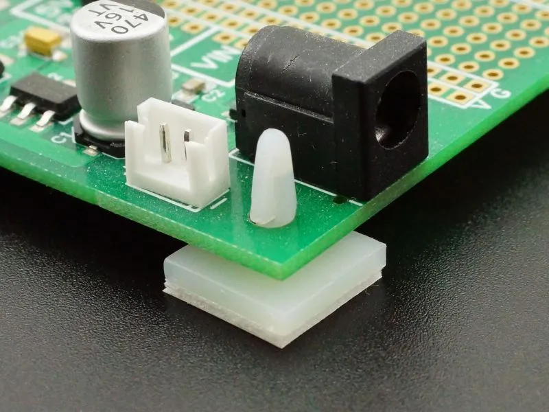
1. Screws and Standoffs
Screws are the most common way to secure a PCB, often paired with standoffs—small spacers that elevate the board above the mounting surface. For a typical PCB thickness of 1.6 mm, use M3 screws (3 mm diameter) with standoffs of 5 mm to 10 mm in height for adequate clearance. This setup is ideal for applications requiring easy removal or replacement.
2. Snap-In Clips
Plastic snap-in clips offer a tool-free mounting solution, snapping into pre-drilled holes. They are lightweight and quick to install, making them suitable for low-stress environments like consumer gadgets.
3. Adhesive Pads
For temporary or lightweight applications, adhesive pads can secure a PCB without drilling holes. However, they are not recommended for high-vibration settings or long-term use due to potential detachment.
4. Rail Systems
In industrial applications, PCBs are often mounted on DIN rails using specialized clips or brackets. This method is common in control systems where multiple boards need to be aligned in a rack.
When choosing hardware, consider factors like weight, environmental conditions (e.g., humidity or temperature extremes), and whether the PCB needs to be removable. For instance, in automotive applications with vibrations up to 10 G, metal screws and standoffs provide the most reliable hold.
Design Tips for PCB Outline and Mounting Holes
Creating a robust PCB design requires attention to detail in both outline and mounting hole planning. Here are actionable tips to ensure your design is both functional and manufacturable:
- Standardize Hole Sizes: Use standard drill sizes (e.g., 3.2 mm for M3 screws) to simplify manufacturing and reduce costs. Non-standard sizes may require custom tools, increasing production time and expense.
- Account for Board Thickness: Ensure the mounting hardware matches the PCB thickness, typically 0.8 mm to 2.4 mm for most designs. Thicker boards may require longer screws or standoffs.
- Reinforce Large Boards: For larger PCBs (over 200 mm in any dimension), add extra mounting holes in the center to prevent flexing. A hole every 100 mm along the length can help distribute stress evenly.
- Use Design Software Features: Most PCB design tools allow you to define mounting holes with specific attributes (plated or non-plated) and integrate them into the mechanical layer alongside the outline. Double-check the output files to ensure accuracy.
- Test Fitment: Before finalizing your design, prototype the PCB and test it with the enclosure and hardware. A small misalignment, even 0.5 mm, can cause assembly issues.
Common Mistakes to Avoid in PCB Outline and Mounting Hole Design
Even experienced designers can make errors when it comes to PCB outlines and mounting holes. Avoiding these common pitfalls can save time, money, and frustration:
- Ignoring Manufacturer Guidelines: Different manufacturers have specific requirements for outline tolerances and hole sizes. Failing to follow these can result in boards that don't fit or can't be mounted correctly.
- Overlooking Stress Points: Placing holes too close to the board edge (less than 2 mm) can weaken the PCB, leading to cracks during assembly or use.
- Forgetting Grounding Needs: If EMI is a concern, ensure at least one mounting hole is plated and connected to the ground plane. Skipping this can degrade performance in high-frequency designs.
- Inconsistent Outline Layers: Ensure the PCB outline is defined on the correct layer in your design software and matches across all related files. Mismatches can lead to manufacturing errors.
Conclusion: Mastering PCB Outline and Mounting Holes for Better Designs
Designing a PCB involves much more than electrical considerations—mechanical aspects like the PCB outline and mounting holes are just as critical to a successful product. A well-planned outline ensures your board fits seamlessly into its enclosure, while strategically placed mounting holes provide the stability and grounding needed for reliable operation. By following the best practices outlined in this guide, such as corner placement for holes, selecting the right hardware, and adhering to clearance rules, you can create PCB designs that are both functional and manufacturable.
Whether you're working on a small hobby project or a complex industrial system, paying attention to these details will elevate the quality of your work. Take the time to plan your outline, position your mounting holes thoughtfully, and choose hardware that matches your application's demands. With these steps, you'll be well on your way to creating robust and professional PCB designs that stand the test of time.


