Mastering Multi Sheet PCB Schematics: A Comprehensive Guide
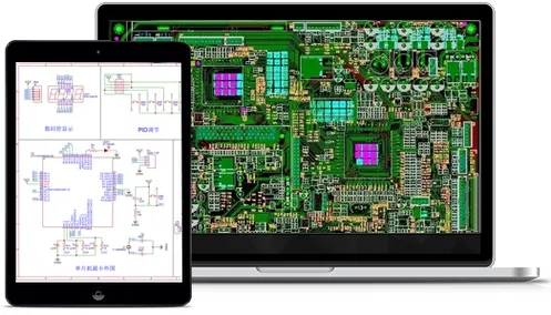
Master multi-sheet schematic PCB and hierarchical schematic design for managing complex PCB schematics and connecting sheets in large projects.
Improve board reliability by using PCB thermal relief to manage heat during soldering. Learn specific spoke patterns that reduce thermal stress and extend the life of your electronic parts.
Adjust Altium Designer thermal relief settings to prevent cold solder joints. Learn to set spoke widths and design rules to manage heat flow through copper pours for reliable PCB assembly.
Discover SMT pad thermal relief design to prevent tombstoning and ensure reliable soldering. Explore thermal balance SMT pads best practices for PCB assembly.
Master PCB grounding techniques to eliminate noise and ground loops. Discover how star grounding and signal integrity strategies ensure reliable performance and stability in your circuit designs.
PCB aspect ratio connects board thickness to via diameter and influences plating reliability. Apply these engineering principles and IPC standards to ensure high quality multilayer manufacturing.
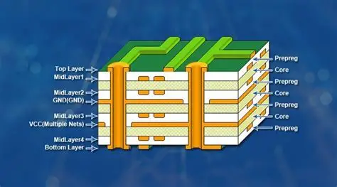
Optimize PCB stack-up designs for aerospace applications in extreme conditions to ensure high-reliability performance in harsh environments.
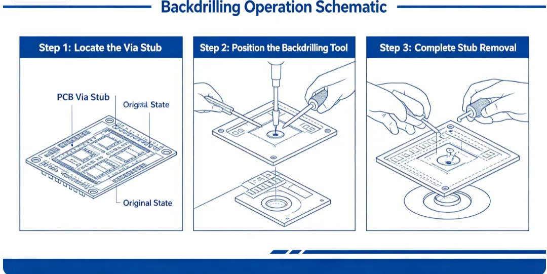
PCB stack up and via design play a key role in maintaining signal integrity in high speed applications. This guide explains how to reduce reflections from via stubs, apply backdrilling, and arrange layers for consistent impedance and reliable performance.
Build a high speed circuit PCB project featuring a signal generator and amplifier. Master impedance control and soldering to ensure clean waveforms and reliability in your custom electronics.
High-speed PCB PCIe Gen5 design balances bandwidth and signal integrity through impedance control, crosstalk reduction, differential pairs, PCB materials, and precise PCIe Gen5 layout. Essential strategies for engineers to achieve reliable 32 GT/s performance in demanding applications.
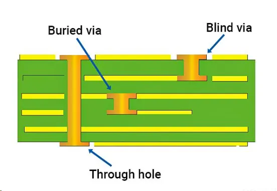
Optimize high speed PCB HDI design to overcome routing density and signal integrity issues. Learn how microvias and blind vias improve stackups and reduce layer counts for superior performance.
High frequency PCB simulation tools help engineers tackle signal integrity, impedance mismatches, and EMI in PCB design. This guide details workflows, best practices, key principles, and troubleshooting for reliable high speed boards used by electrical engineers.
High-frequency PCB backdrilling removes via stubs to improve signal integrity in multilayer boards. This guide covers controlled depth drilling processes, manufacturing steps, key parameters, benefits, challenges, and best practices for electrical engineers working on high-speed designs.
Compare SMT vs through-hole cost, reliability, and advantages for PCB design. SMT excels in density and automation, while through-hole offers mechanical strength for tough environments. Electric engineers get practical best practices, standards guidance, FAQs, and hybrid tips to choose wisely for production success.
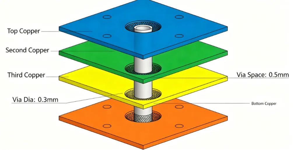
Covers basic via placement guidelines, via types for beginners, via size selection, via spacing rules, and simple PCB via design for electronic hobbyists. Practical tips help create reliable multilayer boards, avoid fabrication issues, and improve prototyping success in PCB design.
Via fence design reduces EMI and crosstalk in sensitive PCB circuits for electric engineers. Details on via fence spacing, via fence grounding, EMI reduction via fencing, and crosstalk prevention via fence. Best practices ensure via fence effectiveness in high-speed multilayer boards to maintain signal integrity.
Create accurate PCB footprints faster with online component libraries. This guide covers PCB footprint databases, component search methods, footprint downloads, and library management practices for electrical engineers to boost design efficiency and ensure standards compliance.
Via tenting process and via plugging process block solder wicking for better PCB reliability. Covers mechanisms, best practices, cost of via tenting, comparisons, troubleshooting, IPC standards, and FAQs for electric engineers.
IPC-7351 compliant component footprints define PCB footprint standards essential for reliable SMT assembly and manufacturing. This guide explains density levels, land pattern design rules, solder joint reliability factors, and component placement accuracy practices to minimize defects and support high yields for engineers.
Via design directly influences signal integrity in high frequency PCBs through stub effects, inductance, and reflections. This guide details backdrilling techniques, blind vias, and optimization strategies to minimize issues and support gigabit speeds for reliable multilayer board performance.