 ALLPCB


Introduction
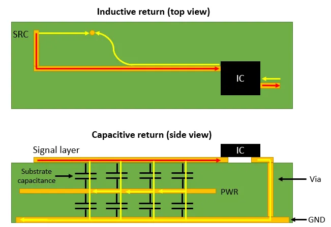
Printed circuit board stack-up design plays a central role in maintaining signal integrity across high-speed electronic systems. Engineers arrange conductive layers, dielectric materials, and reference planes in specific sequences to control impedance, minimize crosstalk, and ensure reliable return paths for signals. Proper layer stackup design directly influences how electromagnetic fields propagate and how noise couples between traces. When signal layers sit adjacent to continuous ground planes, return currents follow low-inductance paths that reduce voltage drops and ringing. Power plane design complements this by providing stable voltage references and aiding in noise suppression when planes are placed strategically near ground layers. These choices become especially critical as data rates increase and board densities rise in modern applications.
What Is PCB Stack-Up Design and Why It Matters
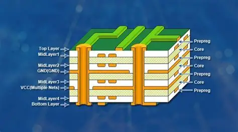
PCB stack-up design refers to the planned sequence and thicknesses of copper layers, prepreg, and core materials that form a multilayer board. This arrangement determines the electrical characteristics of every trace, including characteristic impedance and propagation delay. Industry relevance stems from the need to support faster edge rates while keeping electromagnetic interference within acceptable limits. Signal layer placement decisions affect whether high-speed lines maintain consistent impedance or suffer reflections at discontinuities. Ground plane design ensures every signal has an immediate, low-impedance return path, which limits loop area and radiated emissions. Power plane design further stabilizes supply voltages and supports decoupling strategies when planes are interleaved appropriately. Without careful stack-up planning, even well-routed boards can exhibit excessive jitter, crosstalk, or power integrity issues that compromise overall system performance.
Technical Principles of Layer Arrangement
Effective layer stackup design begins with placing signal layers next to reference planes to establish controlled impedance and tight coupling. A typical configuration alternates signal layers with ground planes so that each high-speed trace sees a uniform dielectric environment above and below. This proximity reduces the loop inductance of the return path and keeps the electric and magnetic fields confined. Ground plane design requires unbroken copper areas that extend under all critical routing channels, avoiding splits that force return currents to detour and create inductive discontinuities. Power plane design follows similar continuity rules, though power planes often incorporate additional features such as stitching vias or segmented regions for different voltage domains. When signal layers are separated from their nearest reference plane by excessive dielectric thickness, impedance rises and crosstalk increases because fringing fields extend farther. Conversely, placing two signal layers between a pair of planes can create broadside-coupled pairs that require precise spacing calculations to avoid excessive coupling. These mechanisms operate according to fundamental electromagnetic principles and align with guidance in IPC-2221 for layout and spacing considerations.
Practical Best Practices for Signal Integrity
Designers achieve reliable PCB stackup signal integrity by following a structured sequence of decisions during the planning phase. First, determine the number of layers needed based on routing density and the number of unique voltage domains. Next, assign the outermost layers as signal layers when possible, or reserve them for components and low-speed signals while dedicating inner layers to high-speed routing between planes. Ground plane design should prioritize solid, unbroken planes on layers immediately adjacent to critical signal layers, with stitching vias placed at regular intervals to maintain continuity across splits. Power plane design benefits from locating power planes adjacent to ground planes so that the pair forms a low-inductance capacitor that aids high-frequency decoupling. Trace widths and dielectric thicknesses are then selected to achieve target impedances, typically 50 ohms single-ended or 100 ohms differential, while maintaining symmetry in the overall build-up to control warpage. Signal layer placement also considers the direction of routing on adjacent layers; orthogonal routing between layers separated by a plane reduces broadside crosstalk. These practices reduce the need for extensive post-layout simulation and help boards meet performance targets on the first fabrication iteration.
Layer-by-Layer Considerations in Complex Designs
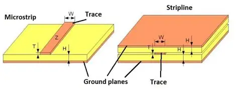
In boards with six or more layers, additional attention to symmetry and material properties becomes necessary. Symmetric stack-ups, where the layer sequence mirrors from top to bottom, minimize mechanical stress during thermal cycling and help maintain flatness. Inner signal layers often use stripline configurations sandwiched between two planes, which provides better shielding than microstrip but requires careful control of dielectric thickness on both sides. Ground plane design in these inner regions must account for via transitions that can interrupt the plane; antipads around vias are sized to balance impedance control with manufacturability. Power plane design may include multiple planes at different voltages, each paired with its own ground reference to keep return paths local. When high-speed differential pairs traverse multiple layers, consistent reference planes on either side of the transition maintain the intended odd-mode impedance. These layer-specific choices collectively determine whether the finished board supports the intended data rates without excessive bit-error rates.
Conclusion
Stack-up design forms the foundation upon which all subsequent routing and component placement decisions rest. By prioritizing adjacent reference planes for every signal layer, maintaining continuous ground and power planes, and selecting appropriate dielectric thicknesses, engineers establish the electrical environment required for clean signal transmission. These principles scale across board complexities and remain consistent with established industry practices. When applied systematically, they reduce the incidence of signal integrity problems that would otherwise require costly respins or extensive mitigation measures.
FAQs
Q1: How does PCB stackup signal integrity improve with proper layer stackup design?
A1: Proper layer stackup design places high-speed signal layers adjacent to continuous ground planes, creating low-inductance return paths that minimize reflections and crosstalk. This arrangement maintains consistent characteristic impedance along traces and reduces electromagnetic interference. Engineers achieve these benefits by following systematic plane assignments that align with IPC-2221 guidance on layout and spacing. The result is cleaner eye diagrams and lower bit-error rates in high-speed interfaces.
Q2: What factors influence signal layer placement in multilayer boards?
A2: Signal layer placement depends on routing density, required impedance targets, and the need for shielding from adjacent layers. Designers typically route critical signals on layers immediately next to ground planes to ensure tight coupling and controlled return paths. Orthogonal routing on layers separated by planes further reduces crosstalk. These choices also consider via transitions and the overall symmetry of the stack-up to maintain mechanical stability.
Q3: Why is ground plane design critical for power integrity as well as signal integrity?
A3: Ground plane design provides the reference for both signal return currents and power distribution networks. Continuous planes minimize voltage drops and inductive noise that can couple into sensitive signals. When power planes sit adjacent to ground planes, the structure forms distributed capacitance that supports high-frequency decoupling. This dual role makes unbroken ground planes essential in any stack-up intended for mixed-signal or high-speed applications.
Q4: How does power plane design interact with signal layer placement?
A4: Power plane design supplies stable voltages while also serving as a reference for some signal layers when ground planes are not adjacent. Placing power and ground planes close together reduces the loop area for supply currents and aids noise suppression. Signal layers routed between or beside these planes experience more stable reference voltages and lower impedance discontinuities. Careful assignment of these layers prevents power noise from modulating signal edges.
References
IPC-2221 — Generic Standard on Printed Board Design. IPC
IPC-6012E — Qualification and Performance Specification for Rigid Printed Boards. IPC, 2017
IPC-A-600K — Acceptability of Printed Boards. IPC, 2020


