ALLPCB


Introduction
Vias serve as vertical interconnects that link different layers in multilayer printed circuit boards. Their placement directly influences electrical performance, thermal dissipation, and overall board reliability. Engineers must consider factors such as layer count, current requirements, and signal frequencies when positioning these structures. Effective via placement PCB techniques reduce parasitic effects while supporting compact layouts. This approach becomes especially important in high-speed digital designs and power electronics applications.
Why Via Placement Matters in PCB Design
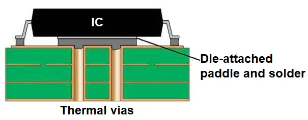
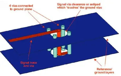
Poor via positioning can introduce unwanted inductance and capacitance that degrade signal quality. Thermal via PCB configurations help transfer heat away from components to inner copper planes or external heatsinks. In contrast, signal via PCB paths must maintain controlled impedance to preserve waveform integrity. Via stitching PCB methods reinforce ground planes and minimize electromagnetic interference across the board. These considerations affect manufacturability as well, since excessive or clustered vias may increase drilling costs and reduce yield during fabrication.
Technical Principles of Via Placement
Vias function as conductive barrels formed by plating drilled holes through the substrate. The aspect ratio of hole diameter to board thickness determines plating uniformity and mechanical strength. Parasitic inductance rises with via length and falls with larger diameters or multiple parallel vias. Thermal resistance decreases when additional vias connect hot components to large copper areas. Capacitive coupling between adjacent vias can create crosstalk if spacing falls below recommended minimums. Current-carrying capacity depends on copper thickness, via diameter, and the number of vias sharing the load. These electrical and thermal mechanisms interact with board stackup, material properties, and operating environment.
Best Practices for PCB Via Optimization
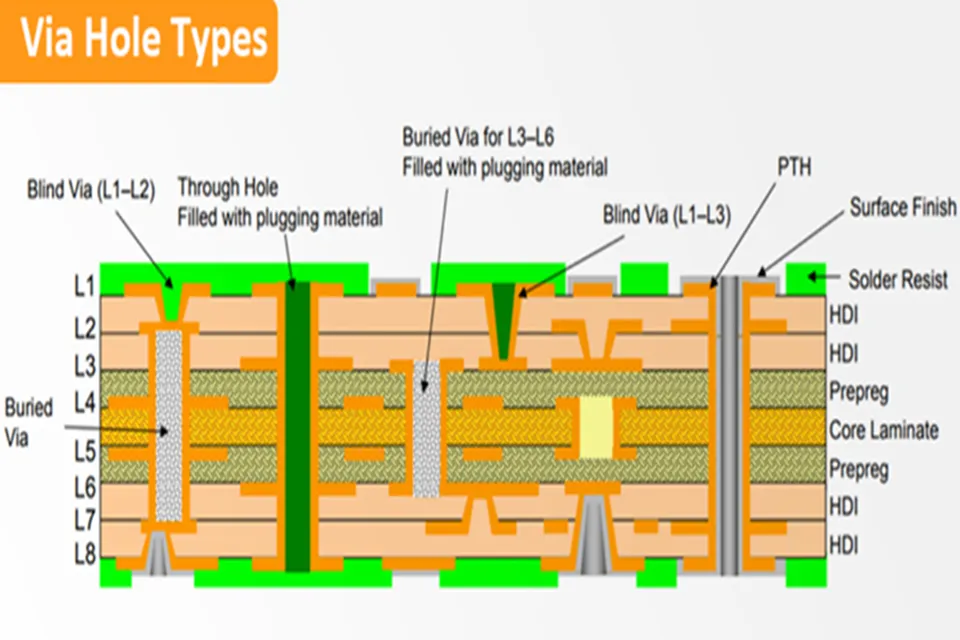
Designers begin by minimizing the total number of vias through careful layer assignment and component placement. When vias are required, they should be distributed evenly rather than clustered to avoid localized stress and manufacturing issues. For high-current paths, multiple thermal via PCB arrays connect power planes and dissipate heat effectively. Signal via PCB transitions benefit from back-drilling or controlled-depth drilling to shorten the unused stub length in high-speed circuits. Via stitching PCB patterns around connectors and along board edges improve return paths and shielding. Spacing rules typically follow at least one via diameter plus clearance for reliable etching and plating. IPC-2221 provides foundational guidance on these dimensional and electrical requirements for printed board design.
Engineers evaluate via-in-pad options only when board real estate is severely limited, because they require additional planarization steps. Aspect ratios should stay within limits that ensure complete plating, commonly below 10:1 for standard processes. Placement near board edges or in high-flex areas requires extra margin to prevent cracking during assembly or operation. Simulation tools help verify that proposed via patterns meet target impedance and thermal profiles before committing to fabrication.
Practical Considerations for Manufacturing and Reliability
Via placement decisions must align with fabrication capabilities outlined in standards such as IPC-6012E. This specification defines acceptance criteria for hole quality, plating thickness, and structural integrity. Overly dense via fields can cause resin starvation or delamination during lamination. Thermal cycling tests reveal that properly spaced vias maintain electrical continuity better than tightly grouped arrangements. Designers therefore review drill maps and copper balancing early in the layout process.
Conclusion
Strategic via placement PCB optimization balances electrical, thermal, and mechanical requirements within the constraints of available manufacturing processes. Thoughtful distribution of signal via PCB, thermal via PCB, and via stitching PCB structures supports reliable performance across diverse applications. Adherence to established design principles reduces the risk of field failures while controlling production costs. Engineers who integrate these considerations from the schematic stage onward achieve more robust and efficient layouts.
FAQs
Q1: What defines effective via placement PCB in multilayer boards?
A1: Effective via placement PCB involves positioning interconnects to minimize inductance, control impedance, and support heat flow while respecting manufacturing limits. Engineers evaluate layer transitions, current density, and return paths during layout. Proper spacing and sizing prevent plating defects and ensure long-term reliability according to accepted industry practices.
Q2: How does PCB via optimization improve signal integrity?
A2: PCB via optimization reduces stub lengths, parasitic capacitance, and impedance discontinuities that distort high-speed signals. Techniques such as back-drilling and strategic ground referencing maintain clean transmission characteristics. These steps become critical when data rates increase and rise times shorten.
Q3: When should thermal via PCB arrays be used?
A3: Thermal via PCB arrays transfer heat from surface-mounted components to inner planes or external cooling structures. They prove useful under power devices or in dense layouts where airflow is restricted. Multiple vias in parallel lower thermal resistance without requiring larger board areas.
Q4: What role does via stitching PCB play in EMI control?
A4: Via stitching PCB connects ground planes at frequent intervals to create low-impedance return paths and contain electromagnetic fields. This technique reduces radiation from board edges and improves shielding effectiveness around sensitive circuits. Consistent stitching patterns help meet electromagnetic compatibility goals.
References
IPC-2221B — Generic Standard on Printed Board Design. IPC, 2012
IPC-6012E — Qualification and Performance Specification for Rigid Printed Boards. IPC, 2017