 ALLPCB


Trace routing forms the backbone of any printed circuit board design. Engineers must balance electrical performance, thermal management, and manufacturability when defining paths for signals and power. Effective trace routing PCB practices directly influence signal integrity, power delivery, and overall board reliability. Poor routing decisions often lead to crosstalk, excessive voltage drop, or thermal hotspots that compromise function. Optimized layouts reduce the need for rework during prototyping and production.
Why Trace Routing Matters in Modern PCB Design
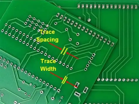
Trace routing PCB decisions affect every aspect of board operation. Signal routing techniques determine whether high-speed data travels cleanly or suffers from reflections and attenuation. PCB trace width and PCB trace spacing control current capacity and isolation between conductors. In dense layouts, these parameters also influence electromagnetic compatibility and heat dissipation. Designers who master these elements create boards that meet performance targets while remaining economical to manufacture.
Industry standards such as IPC-2221 guide the calculation of trace dimensions based on current and temperature rise. Proper application of these guidelines helps avoid both under-sizing, which causes overheating, and over-sizing, which wastes board space. Consistent routing practices also improve yield during fabrication and assembly.
Core Engineering Principles Behind Trace Routing
Current-carrying capacity depends primarily on trace width, copper thickness, and allowable temperature rise. Wider traces reduce resistance and voltage drop but consume more routing area. Conversely, narrow traces suit low-current signals yet require careful thermal analysis. PCB trace optimization therefore begins with accurate current estimates for each net.
Spacing between traces prevents arcing and reduces capacitive coupling. Minimum distances vary with voltage, environmental conditions, and desired insulation resistance. High-voltage circuits demand greater PCB trace spacing than low-voltage digital lines. In mixed-signal boards, additional separation or shielding helps maintain signal integrity across domains.
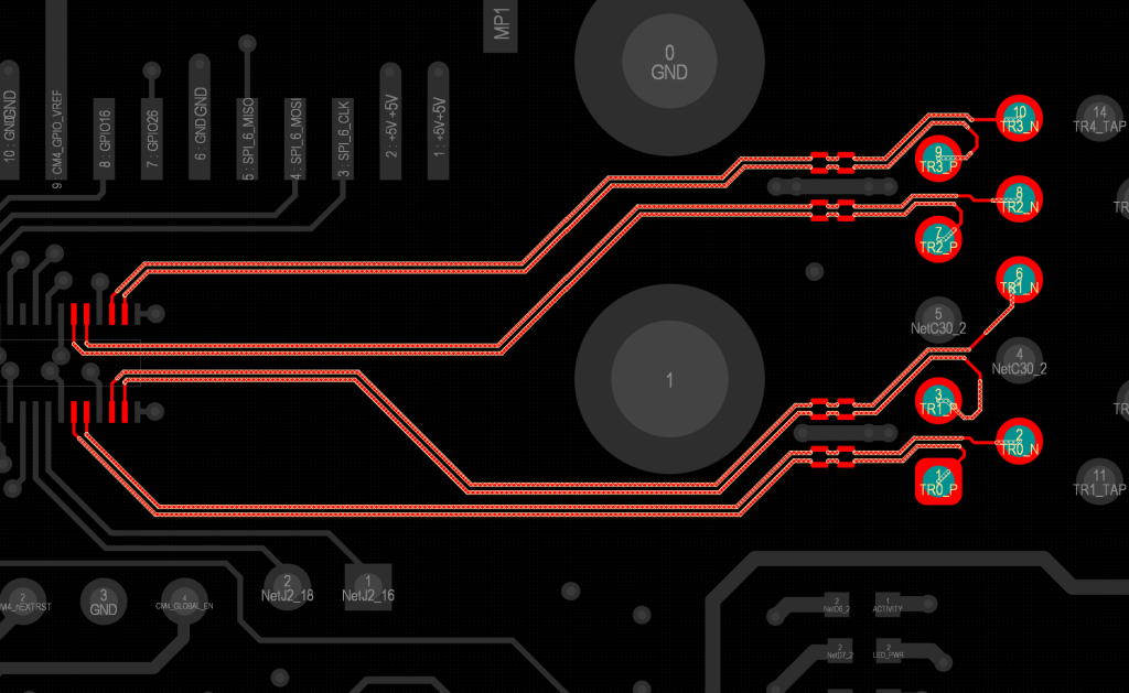
Impedance control adds another layer of complexity for high-speed signals. Trace geometry, dielectric properties, and reference plane proximity must combine to achieve target impedance values. Differential pairs require matched lengths and consistent spacing to preserve signal quality. Deviations in any of these parameters can degrade eye diagrams or increase bit-error rates.
Thermal considerations extend beyond simple width calculations. Heat spreads along traces and through vias, so routing must account for localized power dissipation. Placing high-current traces on outer layers with access to airflow or heatsinks often improves reliability compared with inner-layer routing.
Practical Techniques for Effective PCB Trace Optimization
Begin layout with a clear stack-up definition that assigns signal, power, and ground layers. This foundation supports controlled impedance and provides return paths that minimize loop inductance. Route critical signals first, keeping them short and direct while avoiding unnecessary vias that introduce inductance.
Use 45-degree angles or gentle curves instead of sharp 90-degree corners. Sharp bends concentrate electric fields and can create manufacturing challenges. When routing differential pairs, maintain consistent spacing and length matching within tight tolerances. Serpentine patterns compensate for length differences without introducing excessive skew.
For power distribution, employ wider traces or copper pours sized according to expected current. Multiple vias at transitions between layers reduce resistance and improve thermal conduction. PCB trace spacing around high-voltage areas should exceed minimum requirements when possible to provide design margin.
Review the entire layout for potential coupling issues. Parallel runs of sensitive signals should be minimized, or separated by ground traces or planes. Where crossing is unavoidable, route at right angles to reduce capacitive interaction. Simulation tools help validate these choices before fabrication.
Best Practices for Reliable Signal Routing Techniques
Adopt a systematic approach that starts with schematic-level net classification. Identify high-speed, high-current, and sensitive analog nets early so routing priorities can be assigned accordingly. Follow established design rules derived from IPC-2221 and related documents for width and spacing calculations.
Iterate the layout through multiple reviews focused on different aspects: first electrical performance, then manufacturability, and finally thermal behavior. Small adjustments in trace width or spacing during these reviews often resolve issues that would otherwise appear during testing. Document decisions so future revisions maintain the same performance level.
Consider via placement and pad geometry as integral parts of trace routing. Vias add inductance and resistance, so their use should be minimized on critical paths. When vias are necessary, select appropriate sizes and finishes that support the required current without excessive heat generation.
Conclusion
Mastering trace routing PCB techniques requires attention to width, spacing, impedance, and thermal factors from the earliest design stages. Structured application of signal routing techniques produces layouts that deliver reliable performance while supporting efficient manufacturing. Consistent PCB trace optimization reduces risk and supports the demanding requirements of contemporary electronic systems.
FAQs
Q1: What determines the correct PCB trace width for a given current?
A1: Trace width is calculated from the required current, allowable temperature rise, copper thickness, and ambient conditions. Standards such as IPC-2221 provide charts and equations that translate these inputs into minimum dimensions. Designers often add margin to account for manufacturing tolerances and long-term reliability.
Q2: How does PCB trace spacing affect signal integrity?
A2: Adequate spacing reduces capacitive and inductive coupling between adjacent traces. Insufficient spacing can cause crosstalk that corrupts high-speed signals or triggers false switching in digital circuits. Proper spacing also supports voltage isolation and helps meet electromagnetic compatibility goals.
Q3: Why is length matching important in differential pair routing?
A3: Length matching keeps the two signals in a differential pair arriving at the receiver with minimal skew. Excessive mismatch converts differential signals into common-mode noise and degrades timing margins. Careful routing with serpentine adjustments achieves the required matching while preserving impedance continuity.
Q4: What role does layer stack-up play in trace routing optimization?
A4: The stack-up defines reference planes and dielectric thicknesses that control impedance and provide return paths. A well-chosen stack-up allows tighter spacing on inner layers while maintaining signal integrity. It also influences thermal performance by determining how heat conducts through the board.


