 ALLPCB


Electromagnetic interference, or EMI, can disrupt the operation of electronic devices and cause products to fail regulatory requirements. Engineers must address EMI early in the design process to ensure reliable performance and market access. This guide outlines a structured approach to achieving EMI compliance through careful planning, layout practices, and verification steps. Following established engineering principles helps minimize risks associated with radiated and conducted emissions.
Why EMI Compliance Matters in Product Development
EMI compliance ensures that a product neither generates excessive interference nor becomes susceptible to external disturbances. Regulatory bodies require adherence to limits set by international standards to protect the electromagnetic environment. Non-compliance can result in delayed product launches, costly redesigns, or restricted sales in key markets. For electric engineers working on complex systems, integrating EMI considerations from the concept stage supports both performance goals and regulatory approval.
Core Technical Principles of EMI and EMC
EMI arises from unintended electromagnetic energy generated by switching circuits, clocks, and power converters. This energy couples to other circuits through conduction along traces or radiation through space. Common mechanisms include differential-mode and common-mode currents that excite antenna-like structures on the board. Proper grounding, shielding, and filtering interrupt these paths before they become problematic. Understanding signal integrity alongside EMI behavior allows designers to balance speed requirements with emission control.
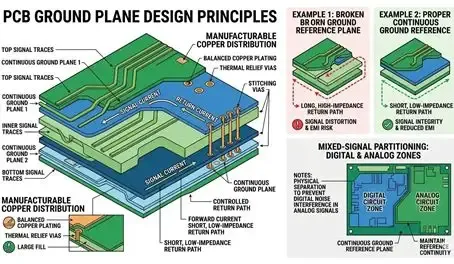
Designers often separate high-speed digital sections from sensitive analog areas to reduce coupling. Decoupling capacitors placed close to integrated circuits provide low-impedance paths for high-frequency currents. Trace routing that minimizes loop areas further limits magnetic field generation. These principles align with practices described in IEC standards for electromagnetic compatibility.
Step-by-Step EMI Compliance Design Process
Begin by defining the operating environment and applicable emission limits during the requirements phase. Identify potential sources such as processors, power supplies, and wireless modules. Create a preliminary layout that groups similar functions and maintains adequate separation between noisy and quiet zones. Select components with known emission characteristics and include filtering at power entry points.
During detailed PCB layout, route critical signals on inner layers where possible and use ground planes to provide return paths. Implement controlled impedance for high-speed lines to reduce reflections. Add stitching vias around board edges and around sensitive circuits to contain fields. Review the design iteratively with simulation tools focused on both signal integrity and radiated emissions.
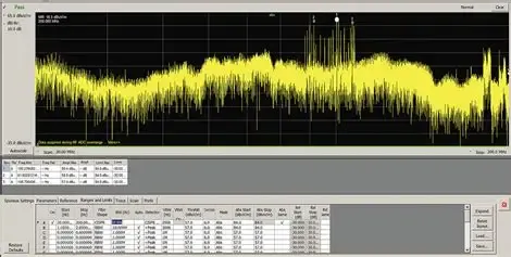
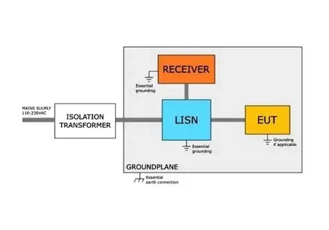
Pre-compliance testing EMI should occur before final prototypes are complete. Measure conducted emissions on power and signal lines as well as radiated emissions in a controlled environment. Compare results against target limits and adjust layout or add suppression components as needed. This early verification reduces the likelihood of failures during formal certification.
Selecting an EMI Test Lab and Completing Regulatory Compliance
Choose a test facility with experience in the product category and the specific standards required for the target markets. Confirm that the laboratory maintains accreditation for the relevant test methods. Provide the lab with detailed documentation including block diagrams, PCB layouts, and operating modes. Schedule testing after the design has passed internal pre-compliance checks to optimize time and cost.
Regulatory compliance EMI typically involves standards such as those in the CISPR family for information technology and multimedia equipment. Document all test configurations and results thoroughly for submission to certification bodies. Address any non-conformances through targeted modifications rather than broad changes that could affect other performance aspects.
Best Practices for Ongoing EMI Control
Maintain consistent grounding strategies across revisions and document all changes that could affect emissions. Use ferrite beads or common-mode chokes only where measurements confirm a benefit, avoiding unnecessary insertion loss. Perform periodic reviews of component availability to ensure substitute parts maintain similar EMI characteristics. These habits support long-term product reliability and simplify future certifications.
Conclusion
A methodical EMI compliance design guide approach integrates layout discipline, component selection, and verification at every stage. Electric engineers who apply these steps early achieve both functional performance and regulatory approval with fewer iterations. Consistent attention to grounding, shielding, and filtering produces robust designs that meet market expectations.
FAQs
Q1: What is the role of pre-compliance testing EMI in the overall EMC design process?
A1: Pre-compliance testing identifies emission issues during development, allowing corrections before formal certification. It reduces risk and cost by confirming that the design meets limits under controlled conditions. Engineers typically perform these checks in-house or at a local facility using simplified setups that correlate well with accredited lab results.
Q2: How do CISPR standards influence EMI compliance design decisions?
A2: CISPR standards define emission limits and measurement methods for various product types. Designers reference these limits when selecting filtering components and determining acceptable board layouts. Early alignment with CISPR requirements streamlines the path to regulatory compliance EMI.
Q3: What factors should guide EMI test lab selection?
A3: Accreditation for the required test methods, experience with similar products, and clear reporting practices are primary considerations. The laboratory should also offer scheduling flexibility and technical support for interpreting results. These elements help ensure accurate data that supports successful certification.
Q4: Why is grounding critical in the EMC design process?
A4: Effective grounding provides low-impedance return paths that minimize loop areas and reduce radiated fields. It also helps isolate different circuit sections to prevent unwanted coupling. Consistent application of grounding techniques across the board supports both emission control and immunity performance.


