ALLPCB


Fanout design plays a central role in modern printed circuit board layouts, particularly when routing signals from high-density components such as ball grid arrays. Engineers must route traces outward from component pads while maintaining signal integrity, managing thermal performance, and controlling overall project expenses. Effective fanout strategies directly influence both fabrication and assembly phases, making cost optimization a key consideration from the earliest design stages. By carefully evaluating material choices, layer counts, and via configurations, design teams can achieve reliable performance without unnecessary expenditure. This approach supports the development of competitive electronic products across consumer, industrial, and automotive sectors.
What Is Fanout Design and Why Cost Optimization Matters
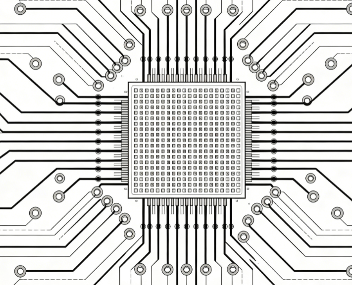
Fanout design refers to the systematic routing of conductive traces from the pads of a surface-mount component to other areas of the board or to vias that connect different layers. In high-pin-count devices, this process often requires multiple vias and careful trace spacing to avoid congestion. Cost optimization in fanout design involves selecting appropriate materials, determining the minimum viable layer count, and planning layouts that reduce both fabrication and assembly expenses. These decisions affect board yield, manufacturing time, and long-term reliability. When executed well, fanout design cost optimization allows engineers to meet electrical and mechanical requirements while staying within budget constraints. Procurement teams and design engineers benefit from understanding these trade-offs early in the project cycle.
Technical Principles of Fanout Design
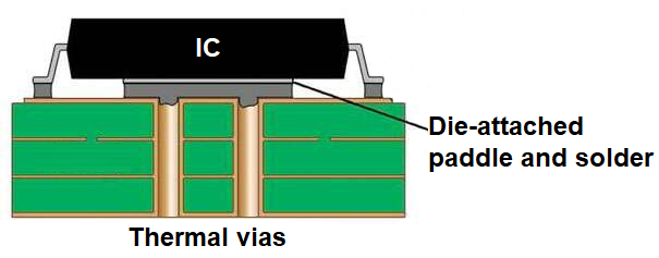
Fanout routing begins with the component footprint and extends outward using a combination of traces and vias. Through-hole vias provide straightforward layer transitions but consume more board space and can increase fabrication cost. Blind and buried vias offer space savings in complex designs yet require additional processing steps during manufacturing. Layer count directly impacts both electrical performance and expense, as each additional layer adds lamination cycles and material usage. Signal integrity considerations, such as controlled impedance and crosstalk reduction, often dictate minimum trace widths and spacing that influence the overall layout density. Thermal management also plays a role, since power distribution planes and heat-spreading features may require dedicated layers or thicker copper weights.
Material selection further shapes the outcome of any fanout strategy. Standard FR-4 laminates provide adequate performance for many applications while keeping material costs moderate. Higher-performance substrates become necessary when operating frequencies demand lower dielectric loss or improved thermal conductivity. The choice of copper weight and surface finish also affects both electrical behavior and assembly compatibility. These technical factors must be balanced against the target operating environment and expected product lifespan. Industry standards such as IPC-6012E guide qualification requirements for rigid printed boards and help ensure consistent quality across different material and layer configurations.
Practical Solutions and Best Practices for Cost Reduction
Design teams can achieve fanout design cost optimization by starting with the minimum layer count that satisfies routing and electrical requirements. Early collaboration between layout engineers and manufacturing partners helps identify opportunities to merge power and ground planes or to use shared vias for multiple signals. Via-in-pad technology can reduce the need for additional escape routing layers, although it requires precise control during fabrication and plating. Material selection should prioritize laminates that meet performance needs without exceeding thermal or frequency specifications. Lower-cost FR-4 variants often suffice for digital and low-to-medium frequency analog circuits, while specialized materials are reserved for radio-frequency or high-speed digital sections.
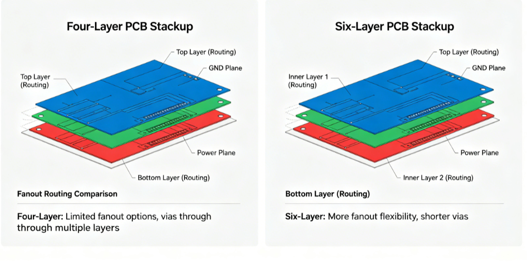
Layer count decisions also influence fanout design fabrication cost. Boards with four to six layers frequently provide sufficient routing resources for many mixed-signal designs when via placement is optimized. Increasing layer count beyond this point raises material and processing expenses disproportionately unless justified by density or impedance requirements. Assembly cost considerations include component placement density, solder paste volume, and board warpage during reflow. Proper pad design and balanced copper distribution help maintain flatness and improve yield during surface-mount assembly. Standards such as JEDEC J-STD-020E provide guidance on moisture sensitivity and reflow profiles that affect assembly reliability and therefore overall project cost.
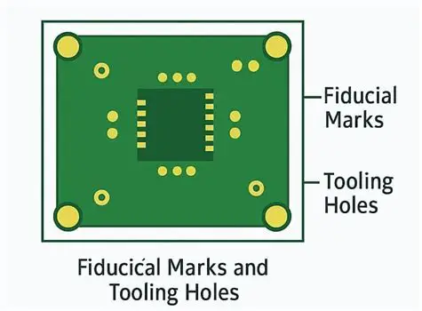
Additional best practices include standardizing via sizes and drill tolerances across the design to simplify tooling and reduce setup charges. Placing test points and fiducials in consistent locations supports automated assembly and inspection processes. When fine-pitch components are involved, careful thermal relief design prevents excessive heat sinking during soldering while preserving electrical performance. These measures collectively lower both fanout design fabrication cost and fanout design assembly cost without compromising functionality.
Conclusion
Cost-effective fanout design requires systematic evaluation of electrical performance, material properties, layer count, and manufacturing processes. Engineers who apply structured analysis to via selection, material choices, and routing density can deliver boards that meet specifications while controlling expenses. Early attention to fabrication and assembly implications prevents costly redesigns later in the project. Consistent application of established industry practices supports repeatable results across multiple production runs. Ultimately, balanced fanout strategies contribute to competitive product development timelines and budgets.
FAQs
Q1: What steps support fanout design cost optimization in high-density layouts?
A1: Engineers begin by determining the minimum layer count required for routing and impedance control. They then evaluate via types and placement to minimize additional processing steps. Material selection focuses on laminates that satisfy electrical and thermal needs without excess cost. These coordinated decisions reduce both fabrication and assembly expenses while preserving signal integrity and reliability.
Q2: How does fanout design material selection influence overall project budget?
A2: Material choice affects dielectric performance, thermal behavior, and manufacturing yield. Standard FR-4 laminates often provide sufficient characteristics for many applications at moderate cost. Higher-performance substrates are used only when frequency or thermal demands require them. Proper selection avoids over-specification and helps control both material purchase price and downstream processing expenses.
Q3: Why does fanout design layer count affect fabrication cost?
A3: Each additional layer increases lamination cycles, material usage, and drilling operations. Four- to six-layer constructions frequently meet routing needs for mixed-signal designs when via placement is optimized. Higher layer counts raise expenses unless justified by density or performance requirements. Early stackup planning helps identify the most economical configuration that still satisfies electrical specifications.
Q4: What considerations reduce fanout design assembly cost?
A4: Assembly cost depends on component placement density, solder joint quality, and board flatness during reflow. Balanced copper distribution and appropriate pad designs help minimize warpage. Consistent via and test point placement supports automated processes and improves first-pass yield. These factors collectively lower labor and rework expenses during surface-mount assembly.
References
IPC-6012E — Qualification and Performance Specification for Rigid Printed Boards. IPC, 2017
JEDEC J-STD-020E — Moisture/Reflow Sensitivity Classification. JEDEC, 2014
IPC-A-600K — Acceptability of Printed Boards. IPC, 2020