ALLPCB


DFA Guidelines and Board Edge Clearance: Preventing Damage During Assembly
Design for assembly practices help engineers create printed circuit boards that move smoothly through manufacturing lines. Board edge clearance forms a key part of these practices because it determines how close components sit to the perimeter of the board. Adequate spacing protects solder joints and board integrity during handling, fixturing, and separation steps. When clearance falls short, mechanical forces can transfer directly to delicate connections and create latent defects that appear only after the product reaches the field.
What DFA Board Edge Clearance Means and Why It Matters
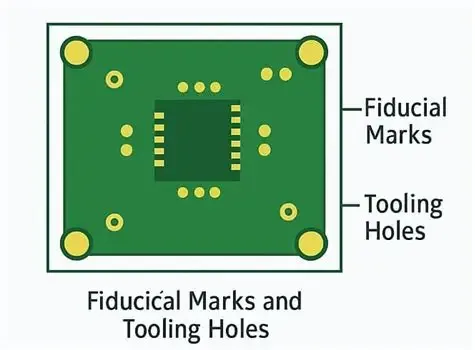
DFA board edge clearance refers to the minimum distance maintained between components and the outer edges of the printed circuit board. This distance also covers areas reserved for tooling holes, fiducials, and clamping zones. Component to edge distance directly influences how the board behaves in automated assembly equipment. Tooling clearance DFA ensures that fixtures and rails can grip the board without contacting active circuitry or mounted parts. Proper clearance reduces the risk of physical damage that leads to cracked solder joints or lifted pads.
Engineers who overlook these margins often encounter higher failure rates during depanelization. Depanelization stress arises when boards are separated from panels through routing, scoring, or snapping. Force applied at the edge travels inward and can fatigue joints located too close to the cut line. Preventing solder joint damage therefore begins at the layout stage rather than during final inspection. Consistent attention to edge margins supports higher first-pass yields and lowers the chance of field returns caused by mechanical stress.
Engineering Mechanisms Behind Edge Clearance Requirements
During panel handling, boards travel through conveyors and placement machines that apply pressure along the edges. Components positioned too near the boundary experience shear or bending moments when the panel flexes. These moments concentrate at the solder fillets and can initiate micro-cracks that propagate under thermal cycling. Tooling features such as registration pins and vacuum cups occupy fixed zones near the perimeter, so components must remain outside those zones to avoid interference.
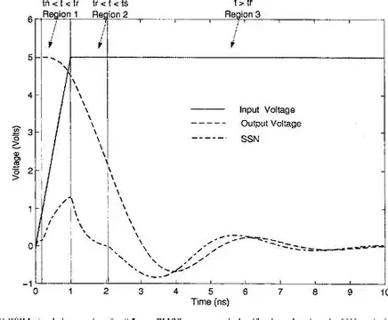
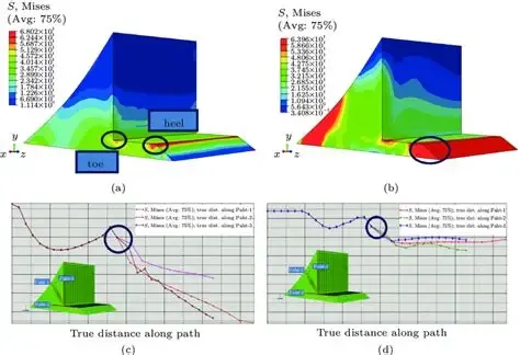
Depanelization introduces additional localized stress. Whether the process uses a router bit or a v-score break, the separation line generates tensile and compressive forces. Joints within the influence zone of these forces absorb part of the energy and may deform. Warpage that develops during reflow can further amplify edge stresses because the board curves and pulls components toward or away from the perimeter. Maintaining sufficient clearance provides a buffer zone that absorbs these movements without transmitting them to the joints.
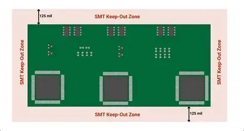
Practical Guidelines for Maintaining Adequate Clearance
Layout teams begin by identifying all mechanical interfaces the board will encounter. These include conveyor rails, fixture clamps, test probes, and depanelization equipment. Each interface defines a keep-out region measured from the board edge inward. Components, traces, and vias stay outside these regions unless specific exceptions receive approval through design review.
Design rules should incorporate separate margins for different assembly stages. Placement clearance accommodates the reach of pick-and-place nozzles. Reflow clearance accounts for board expansion and any fixturing that holds the panel flat. Depanelization clearance provides extra space to isolate joints from cutting forces. Reviewing the entire process flow before finalizing the layout prevents conflicts that appear only on the production floor.
When boards require additional mechanical strength, designers can add non-functional copper or stiffening features near the edges. These features must still respect the clearance zones so they do not create new interference points. Documentation of the chosen margins in the fabrication and assembly drawings allows manufacturers to verify compliance during incoming inspection.
Troubleshooting Common Clearance-Related Issues
When solder joint damage appears near board edges after assembly, the first step is to map the location of failed joints against the original panel routing path. Joints aligned with v-score lines or router entry points often indicate insufficient clearance. Measuring the actual distance from the component body to the final board edge confirms whether the layout met the intended margins.
Another frequent cause involves fixture contact during reflow or wave soldering. If support rails or clamps press against components, the resulting pressure can deform leads or crack fillets. Reviewing fixture drawings against the component placement file reveals overlaps that were not caught during design. Adjusting either the fixture or the component positions restores the required clearance.
In cases where depanelization stress is suspected, engineers can compare boards separated by different methods. Hand snapping typically produces higher localized forces than precision routing. Switching to a gentler separation technique or increasing the clearance distance often resolves recurring edge defects without changing the overall board design.
Conclusion
Board edge clearance forms a foundational element of DFA that protects solder joints throughout the assembly process. By defining keep-out zones for components relative to tooling, handling, and separation lines, engineers reduce mechanical stress and improve long-term reliability. Structured review of each manufacturing step ensures that clearance decisions support both automated production and final product performance.
FAQs
Q1: What is DFA board edge clearance and how does it affect assembly?
A1: DFA board edge clearance defines the minimum distance components must maintain from the board perimeter to avoid interference with fixtures, conveyors, and depanelization equipment. Adequate clearance prevents mechanical forces from reaching solder joints and reduces the likelihood of damage during panel handling and separation.
Q2: How does component to edge distance influence depanelization stress?
A2: Component to edge distance creates a buffer that isolates solder joints from the forces generated when boards are separated from panels. Greater distance allows stress to dissipate before it reaches the joints, lowering the chance of cracks or deformation caused by routing or breaking operations.
Q3: Why is tooling clearance DFA important for preventing solder joint damage?
A3: Tooling clearance DFA reserves space along the board edges for clamps, pins, and rails used in assembly equipment. Without this space, fixtures can press directly on components and transfer pressure to the joints, resulting in immediate or latent damage that appears after thermal cycling.
Q4: What steps help maintain proper clearance throughout the design process?
A4: Design teams identify all mechanical interfaces early, establish keep-out regions for each stage of assembly, and document the margins in fabrication drawings. Regular cross-checks between layout files and equipment specifications catch conflicts before production begins and support consistent quality.
References
IPC-6012E - Qualification and Performance Specification for Rigid Printed Boards. IPC, 2017
IPC-A-600K - Acceptability of Printed Boards. IPC, 2020
JEDEC J-STD-020E - Moisture/Reflow Sensitivity Classification. JEDEC, 2014