ALLPCB


Electronic hobbyists frequently design custom printed circuit boards for projects ranging from simple sensor interfaces to more complex microcontroller systems. Determining the correct trace width ensures that conductors can carry the required current without excessive heating or voltage drop. Creating a personal calculator provides full control over input parameters and output formats while aligning with established engineering practices. This approach supports iterative design adjustments directly on a computer without relying on external software packages. Hobbyists gain practical experience in applying thermal and electrical principles during the layout process.
Why Trace Width Calculation Matters in PCB Design
Proper trace sizing prevents overheating that could damage components or degrade board performance over time. In hobby projects, power traces for motors, LEDs, or power supplies often carry higher currents than signal lines, making accurate calculations essential. Undersized traces lead to temperature rises that violate safety margins, while oversized traces consume unnecessary board space and increase material costs. For electronic hobbyists working on prototypes, reliable calculations help achieve functional boards on the first or second fabrication run. This reduces waste and supports sustainable practices by minimizing failed iterations.
Industry standards guide these decisions to ensure consistency across designs. Calculations typically consider current load, allowable temperature rise, copper thickness, and whether the trace is on an external or internal layer. Following such guidelines helps hobbyists produce boards that perform reliably under real operating conditions.
Technical Principles Behind Trace Width Calculations
Trace width determination relies on the relationship between current flow, conductor cross-section, and heat dissipation. The cross-sectional area of a trace, determined by its width and copper thickness, directly influences its resistance and resulting temperature increase. External traces benefit from better convection cooling compared to internal traces buried within the board stackup. Copper thickness, commonly expressed in ounces per square foot, affects the overall current-carrying capacity for a given width.
Formulas derived from extensive testing relate these variables to predict temperature rise above ambient. Key inputs include the target current in amperes, maximum acceptable temperature increase in degrees Celsius, and board-specific factors such as dielectric thermal conductivity. These relationships allow designers to solve for the minimum required trace width or verify an existing layout.
Reference to established standards appears in technical resources to validate the underlying models. IPC-2152 provides detailed guidance on current-carrying capacity for printed board conductors, incorporating variables like trace location and board construction. This standard improves upon earlier charts by accounting for additional thermal influences present in modern multilayer designs.
Building an Excel PCB Trace Width Calculator
An Excel-based tool offers a straightforward way for hobbyists to implement trace calculations using built-in functions and lookup tables. Begin by creating a new spreadsheet with clearly labeled input cells for current, temperature rise, copper weight, and layer type. Use separate columns or sheets to store reference data points derived from standard charts, allowing the spreadsheet to interpolate or select appropriate values.
Formulas can then combine these inputs to compute the required trace width. For example, arrange cells so that changing the current value automatically updates the output width through arithmetic operations or conditional logic. Add error-checking formulas to flag unrealistic inputs, such as negative currents or excessive temperature rises. This setup enables quick what-if scenarios, such as comparing external versus internal trace requirements for the same current.
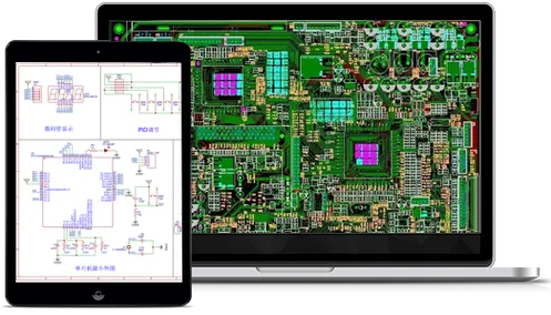
Color-code cells for inputs, calculations, and outputs to improve readability during extended design sessions. Include a simple chart that plots width versus current for visual confirmation of trends. Saving the file as a template allows reuse across multiple projects while preserving the structure.
Developing a Python Script for Trace Width Calculation
Python provides flexibility for hobbyists who prefer scripting or integration with other design workflows. A basic script accepts user inputs through the console or a simple graphical interface and applies the same thermal relationships used in spreadsheet tools. Define functions that encapsulate the calculation logic, accepting parameters like current, temperature rise, and copper thickness before returning the computed width.
The script can incorporate conditional branches to handle external and internal traces differently, reflecting their distinct cooling characteristics. Output results in a formatted table or export them directly to a CSV file for further analysis. Hobbyists can extend the script to process multiple traces in batch mode, reading from a list of requirements and generating a summary report.
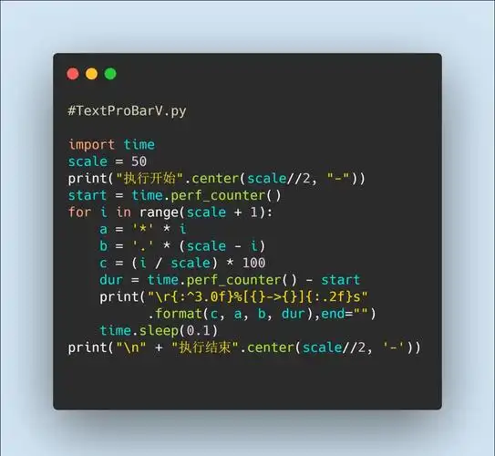
Version control the script using a local repository to track modifications as design needs evolve. This approach supports open source pcb design tools by allowing community contributions or personal customizations without proprietary dependencies.
Practical Best Practices for Custom Calculators
When creating your own tool, validate outputs against known reference cases before applying them to critical traces. Cross-check a few sample calculations manually using the relationships outlined in relevant standards to confirm accuracy. Account for additional factors such as trace length, which influences voltage drop, and nearby heat sources that may affect local temperatures.
For multilayer boards, consider the impact of adjacent copper planes that can act as heat sinks. Test the calculator with a range of realistic hobbyist scenarios, including low-current signal lines and higher-current power distribution. Document any assumptions made in the implementation so that future revisions remain consistent.
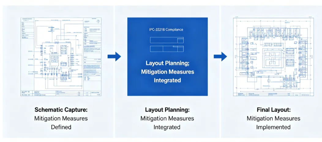
Reference to design standards appears again when reviewing completed layouts. Guidelines from IPC-2221 address broader aspects of conductor sizing within overall board design, complementing the focused current-capacity data. This ensures the calculator supports compliant results without overcomplicating the user interface.
Conclusion
Developing a personal trace width calculator empowers electronic hobbyists to make informed decisions during PCB layout. Whether implemented in a spreadsheet or through scripting, the process reinforces understanding of thermal and electrical trade-offs. Consistent application of these tools leads to more reliable prototypes and efficient use of board real estate. Experimenting with different input combinations reveals practical limits and opportunities for optimization in custom designs.
FAQs
Q1: How does an excel pcb trace width calculator help hobbyists avoid common layout errors?
A1: An excel pcb trace width calculator allows direct entry of project-specific values such as current and temperature rise, producing immediate width recommendations. This interactive format supports rapid adjustments during the design phase and helps maintain consistency across multiple traces on a single board. Hobbyists can save versions for different projects while reviewing the underlying formulas for educational insight.
Q2: What advantages does a python script trace width calculation offer over manual methods?
A2: A python script trace width calculation automates repetitive computations and enables batch processing of multiple traces from a data file. The script can incorporate additional logic for layer type or copper weight, reducing the chance of arithmetic mistakes. Hobbyists benefit from easy modification of the code to include new parameters as their designs become more advanced.
Q3: Are open source pcb design tools suitable for creating custom trace calculators?
A3: Open source pcb design tools provide frameworks that hobbyists can extend with personal calculation modules for trace sizing. These environments support integration of scripts or data exports, allowing seamless workflow from calculation to layout. Users maintain full control over the implementation while benefiting from community-maintained core features.
Q4: Why should designers create pcb design tool solutions tailored to their workflow?
A4: Creating pcb design tool solutions lets hobbyists match the calculator exactly to their preferred inputs, output formats, and project constraints. Custom tools avoid unnecessary complexity found in general-purpose applications and encourage deeper engagement with the underlying engineering principles. This results in designs that better reflect individual experience and specific application requirements.
References
IPC-2152 — Standard for Determining Current-Carrying Capacity in Printed Board Design. IPC, 2009
IPC-2221 — Generic Standard on Printed Board Design. IPC, 2012