ALLPCB


Why Trace Width Matters in PCB Design
Trace width determines the current-carrying capacity of a conductor on a printed board. Narrower traces increase electrical resistance, which generates more heat under load according to basic Joule heating principles. Industry standards such as IPC-2221 provide guidance on minimum widths based on copper thickness, allowable temperature rise, and environmental factors. When designers select widths below these recommendations, boards may pass functional tests at low currents but overheat during normal or peak operation. Procurement teams and designers must verify trace sizing early to avoid costly revisions later in the product lifecycle.
Technical Mechanisms Behind Trace Overheating
Current flow through a conductor produces heat proportional to the square of the current and the resistance of the path. Resistance rises inversely with cross-sectional area, so an undersized trace concentrates thermal energy in a smaller volume. Copper conductivity and board material thermal properties further influence the rate of temperature increase. Over time, repeated thermal cycling can degrade the copper, cause delamination, or initiate microcracks at the trace edges. These effects compound when adjacent components also dissipate heat, creating localized hot spots that accelerate material aging. Engineers performing case study pcb trace overheating reviews commonly observe discoloration, lifted pads, or complete trace burnout in such locations.
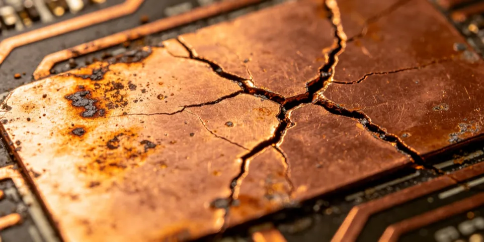
Manufacturing tolerances add another variable. Etching processes can reduce actual trace width below the designed value by several mils. Designers who do not account for these tolerances during layout may discover the shortfall only after boards reach the field. IPC-6012 specifications outline acceptance criteria for conductor width and spacing that help identify such deviations during incoming inspection.
Effects of Incorrect Trace Width on System Reliability
Incorrect trace width produces both immediate and progressive failures. Immediate effects include voltage drops that disrupt sensitive analog circuits or digital signaling margins. Progressive effects appear as intermittent faults that worsen with temperature or load. In high-reliability applications, even brief overheating events can shift component parameters or trigger protective shutdowns. Repairing damaged pcb traces after failure often requires careful removal of charred material, application of conductive epoxy or jumper wires, and verification that the repair restores original current capacity. Without addressing the root sizing issue, repaired boards remain vulnerable to recurrence.

Best Practices for Proper Trace Sizing and Verification
Design teams begin by calculating required widths using established formulas that incorporate maximum current, copper weight, and maximum temperature rise. They then apply a safety margin and review the layout against board stack-up and routing density constraints. Automated design rule checks flag potential violations, yet manual review remains essential for high-current paths and power distribution networks. Post-layout thermal simulation provides additional confirmation before fabrication. During pcb failure analysis trace width examinations, engineers compare measured widths against both design intent and applicable standards to isolate the cause of overheating.
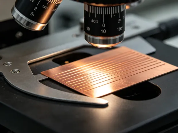
When boards arrive from fabrication, incoming quality control includes spot checks of critical traces. Documentation of actual versus nominal dimensions supports traceability if issues arise later. For existing designs showing symptoms of overheating, systematic current derating or layout revision offers the most reliable long-term solution.
Case Study: Field Failure Attributed to Undersized Power Trace
A power distribution board in an industrial controller exhibited repeated shutdowns after several months of service. Initial visual inspection revealed a darkened trace near a high-current connector. Further pcb failure analysis trace width measurements showed the trace measured 12 mils wide where the design specified 25 mils. Thermal imaging during loaded operation confirmed a hot spot exceeding 120 degrees Celsius. Cross-sectioning revealed copper thinning and void formation consistent with sustained overheating. The root cause traced to an unaccounted etching tolerance combined with an optimistic current estimate during schematic capture. Repairing damaged pcb traces in the returned units involved reinforcing the path with additional copper and updating the design files for future builds. Subsequent units incorporated wider traces and passed extended thermal cycling without recurrence.
Conclusion
Undersized traces represent a preventable source of pcb failure that originates in the design phase yet manifests during operation. Structured application of current-carrying guidelines, tolerance awareness, and verification steps reduces the likelihood of overheating. When failures occur, thorough pcb failure analysis trace width investigation combined with targeted repairs restores functionality while informing design improvements. Consistent attention to these details supports reliable board performance across varied operating conditions.
FAQs
Q1: What role does trace width play in pcb failure analysis trace width investigations?
A1: Trace width directly affects resistance and heat generation. Analysts measure actual widths against design values and standards to determine whether insufficient cross-section contributed to observed overheating or burnout. Accurate measurement helps distinguish design errors from manufacturing variation or external damage.
Q2: How does a case study pcb trace overheating typically unfold in practice?
A2: Engineers first observe symptoms such as intermittent operation or visible discoloration. Thermal imaging locates the hot spot, followed by width measurement and cross-section analysis. The investigation often reveals that the trace carried more current than its dimensions safely allow, confirming the overheating mechanism.
Q3: What are the primary effects of incorrect trace width on board performance?
A3: Incorrect width increases resistance and localized heating, which can cause voltage drops, component stress, or outright trace failure. Over time, thermal cycling may degrade the conductor or surrounding laminate, leading to intermittent faults or permanent damage that requires repairing damaged pcb traces.
Q4: When should designers consider repairing damaged pcb traces versus redesign?
A4: Repair serves as a short-term measure for isolated failures when the root cause is addressed. Redesign becomes necessary when analysis shows the original trace width cannot support required currents under worst-case conditions. Updated layouts incorporate proper sizing and verification steps to prevent recurrence.
IPC-6012E — Qualification and Performance Specification for Rigid Printed Boards. IPC, 2017
IPC-A-600K — Acceptability of Printed Boards. IPC, 2020