 ALLPCB


Navigating the complexities of designing a 4-layer PCB can be challenging, especially when it comes to via placement for optimal signal and power delivery. If you're wondering how to strategically place vias to enhance performance, reduce noise, and maintain impedance, you're in the right place. This guide dives deep into the essentials of via placement in 4-layer PCBs, covering types of vias, stitching techniques, impedance control, and specific strategies for power and signal vias. Whether you're a seasoned engineer or new to PCB design, this comprehensive resource will help you achieve a reliable and efficient design.
Introduction to 4-Layer PCBs and the Importance of Via Placement
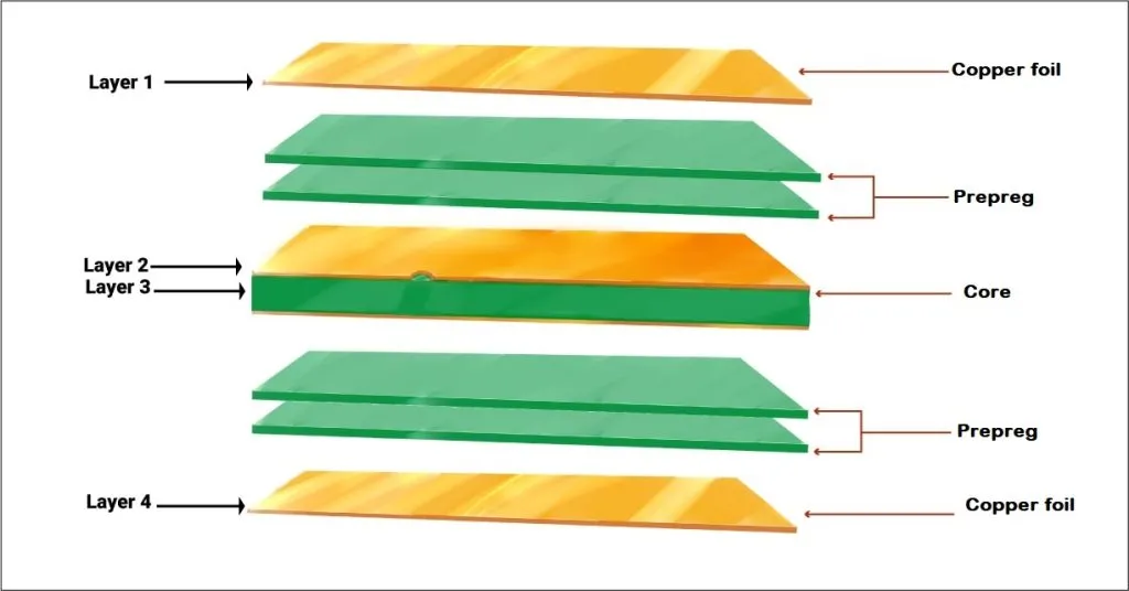
A 4-layer PCB is a popular choice for many electronic designs due to its balance of complexity and cost-effectiveness. With two signal layers (typically top and bottom) and two internal layers often dedicated to power and ground planes, this configuration offers improved signal integrity and power distribution compared to 2-layer boards. However, the placement of vias—small conductive holes that connect different layers—plays a critical role in determining the overall performance of the board.
Vias are not just pathways for signals or power; if placed incorrectly, they can introduce noise, increase impedance mismatches, or disrupt power delivery. Proper via placement ensures minimal signal loss, reduced electromagnetic interference (EMI), and stable power distribution. In this guide, we'll explore the best practices for via placement in 4-layer PCBs, focusing on optimizing both signal and power delivery.
Suggested Reading: 4 layers PCB: Everything You Need to Know
Understanding 4-Layer PCB Via Types
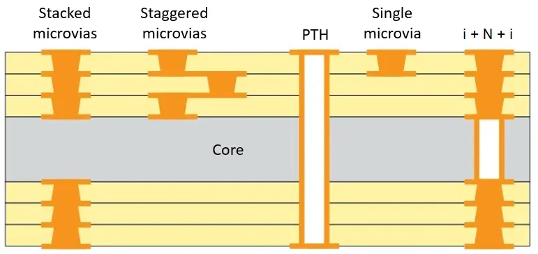
Before diving into placement strategies, it's essential to understand the different types of vias used in 4-layer PCB designs. Each type serves a specific purpose and impacts signal and power delivery differently.
- Through-Hole Vias: These vias extend through all layers of the PCB, connecting components or traces from the top to the bottom. While they are simple to manufacture, they can consume valuable space on internal layers and introduce unnecessary capacitance, which may affect high-speed signals.
- Blind Vias: These connect an outer layer to an inner layer without passing through the entire board. For instance, a blind via might connect the top layer to an internal power plane. They are ideal for saving space but are more expensive to fabricate.
- Buried Vias: Buried vias connect internal layers without reaching the outer surfaces. They are useful for routing signals or power between internal planes but add to manufacturing costs.
- Microvias: These are smaller vias, often used in high-density designs. They typically connect adjacent layers and are crucial for minimizing signal path lengths in high-speed applications.
Choosing the right via type depends on your design requirements, such as signal speed, board density, and budget. For most 4-layer PCBs, a combination of through-hole and blind vias offers a practical solution for balancing cost and performance.
4-Layer PCB Via Stitching: Enhancing Ground and Power Planes
Via stitching is a technique used to connect power or ground planes across layers, improving electrical and thermal performance. In a 4-layer PCB, where internal layers are often dedicated to power and ground, via stitching helps create a low-impedance path for current return and reduces EMI compliance testing.
Why Use Via Stitching? Stitching vias tie together ground planes or power planes, ensuring a consistent reference potential across the board. Without proper stitching, high-frequency signals can create ground loops or voltage drops, leading to noise and signal degradation. Additionally, stitching vias improve thermal dissipation by providing multiple paths for heat to escape.
Best Practices for Via Stitching:
- Place stitching vias around the edges of the PCB to form a "via fence," which helps shield the board from external EMI.
- Position vias near high-current components or areas with significant switching activity to minimize voltage fluctuations.
- Space stitching vias at intervals of about 1/20th of the wavelength of the highest frequency signal on the board. For a 1 GHz signal, this translates to a spacing of roughly 15 mm, though this can vary based on dielectric properties.
- Use a grid pattern for stitching vias on large ground planes to ensure uniform current distribution.
By implementing via stitching effectively, you can significantly enhance the stability of power delivery and signal integrity in your 4-layer PCB design.
Suggested Reading: Beyond the Basics: Advanced Routing Techniques for High-Density 4-Layer PCBs
4-Layer PCB Impedance Control with Vias
Impedance control is critical for high-speed signals in 4-layer PCBs, as mismatches can lead to signal reflections, crosstalk, and data errors. Vias, while necessary for layer transitions, can introduce impedance discontinuities if not managed properly.
How Vias Affect Impedance: A via acts as a small inductor and capacitor in the signal path, altering the characteristic impedance. For a typical microstrip trace with a 50-ohm impedance, a poorly designed via can increase this to 60 ohms or more, causing reflections. The effect is more pronounced at higher frequencies, such as those above 500 MHz.
Tips for Impedance Control with Vias:
- Minimize via length by using blind or microvias for high-speed signals. Shorter vias reduce inductance and maintain impedance closer to the target value.
- Place ground vias near signal vias to provide a return path and reduce loop inductance. A common rule is to place a ground via within 0.5 mm of a high-speed signal via.
- Avoid routing high-speed signals through multiple vias if possible, as each transition adds to impedance mismatch.
- Use simulation tools to model via impedance during the design phase. Adjusting via diameter (e.g., reducing from 0.3 mm to 0.2 mm) or pad size can help match impedance to the trace.
By carefully designing via placement and structure, you can maintain consistent impedance across your 4-layer PCB, ensuring reliable signal transmission even at high frequencies.
4-Layer PCB Power Via Placement: Ensuring Stable Power Delivery
Power delivery is a cornerstone of any PCB design, and in a 4-layer PCB, power vias connect components to internal power planes. Poor placement can lead to voltage drops, noise, and inefficient power distribution.
Key Considerations for Power Via Placement:
- Proximity to Components: Place power vias as close as possible to the power pins of ICs and other high-current devices. This reduces the resistance and inductance in the power path, minimizing voltage drops. For example, placing a via within 0.5 mm of a power pin can reduce IR drop by up to 10% in some designs.
- Decoupling Capacitors: Position power vias near decoupling capacitors to ensure a low-impedance path to the power plane. A common practice is to place a via on each side of the capacitor pad, connecting directly to the power and ground planes.
- Via Sizing: Use larger vias for power connections to handle higher currents. A via with a 0.4 mm diameter can typically carry 1-2 A, but check with PCB manufacturer for specific limits based on copper thickness (e.g., 1 oz or 2 oz).
- Multiple Vias for High Current: For components drawing significant current, such as power regulators, use multiple power vias in parallel to reduce resistance and improve thermal dissipation.
Effective power via placement ensures that your 4-layer PCB delivers stable voltage to all components, even under varying load conditions.
4-Layer PCB Signal Via Placement: Minimizing Signal Loss
Signal vias are used to route traces between layers, often for high-speed or critical signals in a 4-layer PCB. Incorrect placement can degrade signal quality, especially for frequencies above 100 MHz.
Strategies for Signal Via Placement:
- Shortest Path: Place signal vias to create the shortest possible path between layers. For instance, if transitioning from the top layer to an internal signal layer, use a blind via to avoid unnecessary length.
- Return Path: Always provide a nearby ground via for each signal via to maintain a consistent return path. Without this, the signal may couple to unintended paths, increasing crosstalk. A spacing of 0.3-0.5 mm between signal and ground vias is often sufficient.
- Avoid Stub Effects: Unused portions of through-hole vias can act as stubs, causing signal reflections. If a through-hole via is unavoidable, consider back-drilling to remove the stub or use blind vias instead.
- Spacing from Other Signals: Keep signal vias at least 2-3 times the via diameter away from other high-speed signal vias to prevent crosstalk. For a 0.25 mm via, this means a spacing of 0.5-0.75 mm.
By following these guidelines, you can minimize signal loss and maintain integrity across your 4-layer PCB design, even for demanding applications.
Common Mistakes to Avoid in Via Placement
Even with the best intentions, certain pitfalls can compromise via placement in 4-layer PCBs. Here are some common mistakes to watch out for:
- Overusing Through-Hole Vias: Relying solely on through-hole vias can clutter internal layers and disrupt power and ground planes. Use blind or buried vias where feasible.
- Ignoring Thermal Effects: High-current vias can heat up if not sized or spaced properly. Ensure adequate copper around vias to dissipate heat.
- Neglecting Simulation: Failing to simulate via effects on impedance or power delivery can lead to unexpected performance issues. Use design tools to validate placement before fabrication.
- Poor Spacing: Placing vias too close together can cause manufacturing defects or signal interference. Follow design rules for minimum spacing, often around 0.2-0.3 mm for standard processes.
Avoiding these errors will save time and resources while ensuring a robust 4-layer PCB design.
Conclusion: Mastering Via Placement for 4-Layer PCB Success
Via placement in 4-layer PCBs is a critical aspect of optimizing signal and power delivery. From selecting the right via types to implementing stitching techniques, controlling impedance, and strategically placing power and signal vias, every decision impacts the board's performance. By following the best practices outlined in this guide, you can minimize noise, reduce EMI, and ensure stable operation for your electronic designs.
Remember that each project may have unique requirements, so adapt these guidelines to suit your specific needs. With careful planning and attention to detail, your 4-layer PCB can achieve the reliability and efficiency required for modern applications. Start incorporating these via placement strategies into your next design, and watch your PCB performance soar.


