 ALLPCB


Printed Circuit Board (PCB) design is a complex process where precision is paramount. Even a minor oversight in the layout can lead to costly manufacturing defects, signal integrity issues, or outright board failure. This is where Design Rule Check (DRC) comes in—a critical step that validates your PCB layout against predefined manufacturing and design constraints. By catching errors early, DRC ensures your design is functional, reliable, and manufacturable. In this blog, we dive into the essentials of DRC, highlight common PCB layout mistakes, and share practical tips to avoid them, empowering engineers to create high-quality boards.
Whether you're designing a high-speed digital circuit or a compact IoT device, understanding and leveraging DRC can save time, reduce costs, and enhance performance. Let's explore how DRC works, the pitfalls it helps you avoid, and best practices to streamline your PCB design process.
Recommended Reading: Signal Integrity Issues and Solutions in High-Speed PCB Design
What is Design Rule Check (DRC)?
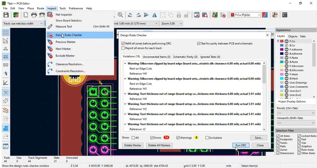
Design Rule Check (DRC) is an automated process within Electronic Design Automation (EDA) software that verifies a PCB layout against a set of predefined rules. These rules, often based on manufacturing capabilities, industry standards, and project-specific requirements, cover parameters like trace widths, clearances, via sizes, and component spacing. By running DRC, designers can identify potential errors before fabrication, minimizing the risk of costly rework.
DRC checks various aspects of the layout, including:
- Geometric constraints: Minimum trace widths, via diameters, and component clearances.
- Electrical rules: Signal integrity, impedance control, and power/ground connectivity.
- Manufacturability: Solder mask clearances, drill hole sizes, and board edge proximity.
For example, a typical DRC rule might specify a minimum clearance of 0.2 mm between traces to prevent short circuits, especially in high-density designs. Running DRC early and often ensures compliance with these constraints, improving yield and reliability.
Why DRC Matters in PCB Design
The complexity of modern PCBs—featuring multilayer boards, high-speed signals, and dense component placement—makes manual verification nearly impossible. A single oversight, like a misaligned via or inadequate solder mask clearance, can lead to manufacturing defects or performance issues. DRC automates this validation, offering several key benefits:
- Early Error Detection: Identifies issues like short circuits or misaligned vias during the design phase, reducing prototype iterations.
- Cost Efficiency: Fixing errors before fabrication avoids expensive rework. For instance, correcting a trace width violation in software is far cheaper than scrapping a batch of faulty boards.
- Improved Manufacturability: Ensures the design aligns with the manufacturer's capabilities, such as minimum drill hole sizes (e.g., 0.3 mm for standard processes).
- Enhanced Reliability: Verifies signal integrity and power distribution, critical for applications like automotive or medical electronics where failure is not an option.
According to industry data, up to 70% of PCB design errors can be caught by running comprehensive DRC checks, significantly boosting first-pass yield.
Common PCB Layout Mistakes DRC Helps Avoid
DRC is a powerful tool for catching a wide range of layout errors. Below, we outline the most common PCB design mistakes and explain how DRC rules can prevent them.
1. Insufficient Trace Clearance
One of the most frequent errors in PCB design is inadequate spacing between conductive elements like traces, pads, or vias. Insufficient clearance can cause short circuits, especially in high-voltage or high-density designs. For example, a clearance of less than 0.15 mm between traces in a 5V circuit may lead to arcing or solder bridging during assembly.
DRC Solution: Set clearance rules based on the board's voltage and manufacturing capabilities. A typical rule might enforce a minimum of 0.2 mm for low-voltage designs and 0.5 mm for higher voltages. DRC flags any violations, allowing you to adjust spacing before finalizing the layout.
2. Incorrect Trace Widths
Trace widths determine a trace's current-carrying capacity and impedance. Undersized traces can overheat or cause voltage drops, while oversized traces waste board space. For instance, a 10-mil (0.254 mm) trace may be insufficient for a 2A current, risking thermal failure.
DRC Solution: Define trace width rules based on current requirements and impedance control. Tools like Altium Designer allow you to specify minimum widths (e.g., 0.3 mm for 1A signals) and check for compliance. DRC also ensures effect trace widths for controlled-impedance traces, critical for high-speed signals like USB (90 Ω differential impedance).
3. Misaligned or Improperly Sized Vias
Vias connect layers in multilayer PCBs, but errors like misaligned vias or incorrect drill sizes can weaken board integrity or cause connectivity issues. For example, a via with a drill diameter smaller than 0.3 mm may be unmanufacturable by some fabricators, leading to open circuits.
DRC Solution: Set rules for via drill diameters (e.g., minimum 0.3 mm) and annular ring sizes (e.g., 0.15 mm minimum). DRC verifies proper alignment and spacing, ensuring vias are robust and manufacturable.
4. Inadequate Solder Mask Clearance
Solder mask clearance is the gap between the solder mask and exposed pads or traces. Insufficient clearance (e.g., less than 0.1 mm) can cause solder bridging during assembly, leading to shorts. This is especially critical in fine-pitch components like QFN packages.
DRC Solution: Define solder mask clearance rules to ensure sufficient spacing. DRC checks for violations, helping you adjust the mask design to prevent assembly issues.
5. Board Edge Proximity Issues
Placing copper features too close to the board edge (e.g., within 0.5 mm) can result in shorts during fabrication when the board is cut. This is a common issue in compact designs where space is at a premium.
DRC Solution: Enforce board edge clearance rules to maintain a safe distance between copper and the board outline. DRC highlights any features that violate this constraint, allowing repositioning.
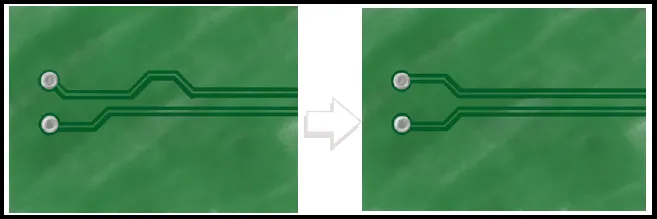
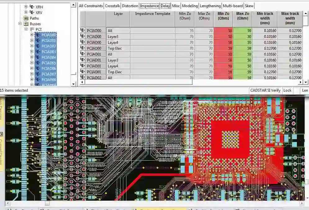
6. Signal Integrity Violations
High-speed designs, such as those involving DDR4 or PCIe, require careful routing to maintain signal integrity. Issues like excessive trace length, improper differential pair spacing, or nets crossing split planes can cause reflections, crosstalk, or EMI. For example, a differential pair with spacing greater than 0.2 mm may fail to maintain 100 Ω impedance.
DRC Solution: Implement rules for differential pair spacing, impedance control, and return path continuity. Advanced DRC tools can flag nets crossing split planes, ensuring a low-impedance return path to minimize EMI.
Best Practices for Running DRC Effectively
To maximize the benefits of DRC, follow these best practices to ensure thorough validation and a smooth design process.
1. Define Rules Early
Configure DRC rules at the start of your project, aligning them with your manufacturer's capabilities and project requirements. For example, check your fabricator's minimum trace width (e.g., 0.15 mm for standard processes) and incorporate it into your EDA tool. Tools like KiCad and Altium Designer allow you to customize rules for clearances, trace widths, and via sizes.
2. Use Online and Batch DRC
Most EDA software offers two DRC modes:
- Online DRC: Runs in real-time during layout, flagging violations as you work. This is ideal for catching errors early, such as incorrect trace spacing.
- Batch DRC: Performs a comprehensive check at the end of the design, generating a detailed report. Always run a batch DRC before generating Gerber files to catch any overlooked issues.
3. Regularly Update Rules
As your design evolves, update DRC rules to reflect changes in requirements, such as tighter tolerances for high-speed signals. For instance, a 10-layer board may require stricter clearance rules (e.g., 0.1 mm) than a 2-layer board.
4. Collaborate with Manufacturers
Work closely with your PCB manufacturer to ensure your DRC rules match their capabilities. For example, confirm minimum annular ring sizes or solder mask tolerances to avoid surprises during fabrication. Many manufacturers provide DRC rule files for tools like KiCad or Allegro, simplifying setup.
5. Review and Resolve Violations
When DRC flags violations, carefully review each one in the context of your design. Some violations may be intentional (e.g., tighter clearances for specific components), but others require correction. Use the EDA tool's navigation features to jump to the exact location of each error, and re-run DRC after making changes to confirm resolution.
Challenges in DRC and How to Overcome Them
While DRC is invaluable, it's not without challenges. Here's how to address common hurdles:
- Balancing Strictness: Overly conservative rules (e.g., 0.5 mm clearance for a low-voltage design) can limit design flexibility, while lenient rules may miss critical errors. Solution: Fine-tune rules based on your project's needs and consult with your manufacturer.
- Time-Intensive Checks: Complex designs with thousands of components can slow down DRC, especially batch mode. Solution: Run DRC on smaller sections of the board during development to save time.
- False Positives: DRC may flag intentional design choices as violations. Solution: Use waiver options in tools like Altium Designer to suppress non-critical alerts, but document these decisions for clarity.
Conclusion
Design Rule Check (DRC) is an indispensable tool for avoiding common PCB layout mistakes, from insufficient clearances to signal integrity violations. By setting up comprehensive rules, running DRC early and often, and collaborating with your manufacturer, you can ensure your designs are manufacturable, reliable, and high-performing. Whether you're tackling a simple 2-layer board or a complex multilayer design, mastering DRC will save time, reduce costs, and elevate your engineering outcomes.
Take the time to define accurate DRC rules, leverage both online and batch checks, and review violations carefully. With these practices, you'll minimize errors and deliver PCBs that meet the demands of today's fast-evolving electronics industry. Start implementing these strategies in your next project, and experience the difference a thorough DRC process can make.


