 ALLPCB


AI is revolutionizing PCB design by automating repetitive tasks, improving accuracy, and enabling engineers to tackle increasingly complex projects. Machine learning (ML) algorithms analyze vast datasets to suggest optimal component placements, predict signal integrity issues, and streamline routing. For instance, AI can reduce trace lengths by up to 20% compared to manual designs, minimizing signal interference and improving performance. These advancements are critical as electronic devices become smaller and more powerful, demanding high-density interconnect (HDI) boards with microvias and fine-pitch components.
Trend 1: AI-Powered Design Optimization
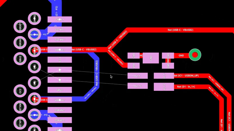
One of the most significant trends in 2025 is the use of AI to optimize PCB layouts. AI algorithms analyze design constraints—such as impedance requirements (e.g., 50 ohms for high-speed signals), thermal dissipation, and board size—to suggest layouts that maximize performance. For example, AI can place components to ensure signal paths are as short as possible, reducing latency in applications like 5G, where data transmission rates exceed 10 Gbps. Tools like Zuken's CR-8000 Design Force use AI to perform real-time constraint-driven routing, cutting design time by up to 30%.
AI also enhances collaboration by providing instant feedback to designers. For instance, if a trace violates a design rule (e.g., minimum spacing of 0.1 mm), AI flags the issue and suggests corrections, reducing costly redesigns. This is particularly valuable for HDI PCBs, where microvias (as small as 0.05 mm) demand precision.
Trend 2: AI for Signal and Power Integrity Analysis
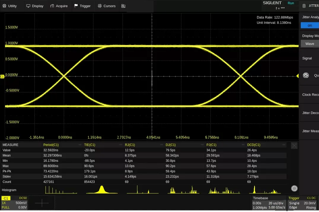
Signal integrity (SI) and power integrity (PI) are critical for high-speed PCBs, especially in applications like automotive radar and IoT devices. AI-driven tools simulate time-domain and frequency-domain effects, such as crosstalk and impedance mismatches, with unprecedented accuracy. For example, AI can predict signal reflections in a 10-layer PCB with a 100 MHz clock speed, ensuring compliance with standards like PCIe 6.0 (64 GT/s). By analyzing eye patterns, AI assesses signal quality, reducing bit error rates to below 10^-12.
Power integrity is equally important, as modern devices require stable voltage supplies (e.g., 1.2V for DDR5 memory). AI optimizes power delivery networks (PDNs) by minimizing voltage drops and reducing electromagnetic interference EMI compliance testing. This results in circuits that consume up to 15% less power, extending device lifespan and supporting sustainability goals.
Trend 3: AI-Enhanced Thermal Management
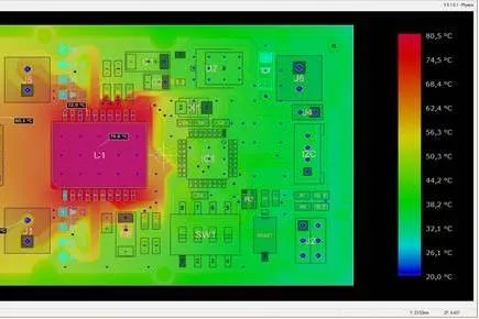
As electronic devices shrink, thermal management becomes a challenge. AI helps engineers design PCBs that dissipate heat efficiently, preventing failures in high-power applications like electric vehicle (EV) chargers. AI algorithms analyze heat distribution across a PCB, recommending materials like metal core PCBs (MCPCBs) with thermal conductivities of 1-4 W/m·K for LED applications. They also suggest optimal via placements to reduce thermal resistance by up to 25%.
For example, in a multi-layer PCB for an EV battery management system, AI can identify hotspots (e.g., near a 100W power module) and propose thermal vias or heat sinks. This ensures components operate within safe temperature ranges (typically below 85°C), improving reliability.
Trend 4: AI in Flexible and Rigid-Flex PCB Design
Flexible and rigid flex PCBs are gaining traction in 2025, driven by demand for lightweight, adaptable electronics in wearables, aerospace, and healthcare. AI optimizes these designs by accounting for mechanical stresses and dynamic bending. For instance, AI ensures that traces on a polyimide substrate maintain integrity during 10,000 bending cycles, critical for medical devices like diagnostic patches.
AI also supports hybrid designs combining rigid and flexible sections. By simulating stress points, AI recommends trace widths (e.g., 0.2 mm) and layer stack-ups to prevent cracking. This trend is fueled by the growing rigid-flex PCB market, expected to grow at a CAGR of 10% from 2023 to 2028.
Trend 5: AI-Driven Sustainability in PCB Design
Sustainability is a priority in 2025, with engineers seeking eco-friendly PCB solutions. AI supports this by recommending biodegradable substrates, such as cellulose-based materials, and optimizing material usage to reduce waste by up to 20%. For example, AI can minimize copper usage in a 4 layer PCB, lowering the environmental impact of etching processes.
AI also enhances energy-efficient manufacturing by predicting equipment maintenance needs, reducing downtime by 15%. Lead-free soldering techniques, optimized by AI, further align with regulations like RoHS, ensuring compliance without compromising quality.
Trend 6: AI for Additive Manufacturing and 3D Printing
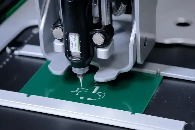
Additive manufacturing, including 3D printing, is transforming PCB prototyping in 2025. AI streamlines the process by generating complex multi-layer designs with embedded components, reducing board size by up to 30%. For instance, AI can design a 3D-printed PCB with integrated diodes and thin-film transistors (TFTs) using organic polymers, ideal for environmental sensors.
AI also reduces material waste in additive manufacturing by optimizing print paths, cutting production costs by 10-15%. This is particularly valuable for rapid prototyping, where engineers need functional boards in days rather than weeks.
Challenges of AI-Driven PCB Design
Despite its benefits, AI-driven PCB design faces challenges. Supply chain issues can delay access to advanced materials like Rogers laminates, which have low dielectric loss (e.g., 0.002 at 10 GHz). Additionally, the high cost of AI tools and training can be a barrier for smaller firms. Quality control remains critical, as AI may overlook nuanced design flaws, requiring human oversight to ensure reliability.
Engineers must also address data security, as AI relies on cloud-based platforms that store sensitive design files. Robust encryption and secure workflows are essential to protect intellectual property.
How ALLPCB Supports AI-Driven PCB Design
At ALLPCB, we empower engineers to leverage AI-driven PCB design trends with our advanced manufacturing capabilities and quick-turn prototyping. Our global logistics network ensures rapid delivery of high-quality PCBs, including HDI and rigid-flex boards, in as little as 24 hours. With state-of-the-art facilities, we support AI-optimized designs by offering precise fabrication for microvias (down to 0.05 mm) and fine-pitch components. Our commitment to sustainability aligns with AI-driven eco-friendly practices, using lead-free soldering and recyclable materials to meet industry standards. Whether you're designing for 5G, IoT, or automotive applications, ALLPCB provides the tools and expertise to bring your AI-optimized PCBs to life.
Conclusion
AI is transforming PCB design in 2025, enabling engineers to create smaller, more efficient, and sustainable boards for cutting-edge applications. From optimizing layouts and ensuring signal integrity to enhancing thermal management and supporting additive manufacturing, AI-driven trends are reshaping the industry. By staying informed about these advancements and partnering with reliable manufacturers, engineers can overcome challenges and deliver innovative electronics. As we continue to push the boundaries of PCB design, AI will remain a cornerstone of progress, driving performance and sustainability in equal measure.


