 ALLPCB


In the world of PCB design, achieving higher density without sacrificing performance or reliability is a constant challenge. Via-in-Pad (VIP) technology offers a powerful solution for high-density PCB designs by allowing vias to be placed directly within component pads. This approach saves valuable board space and improves signal integrity. In this comprehensive guide, we’ll dive into Via-in-Pad Design for Manufacturability (DFM), covering essential topics like design guidelines, manufacturing processes, reliability concerns, thermal management, and cost analysis. Whether you're an experienced engineer or new to high-density designs, this blog will provide actionable insights to optimize your projects.
What is Via-in-Pad and Why Use It for High-Density PCB Designs?
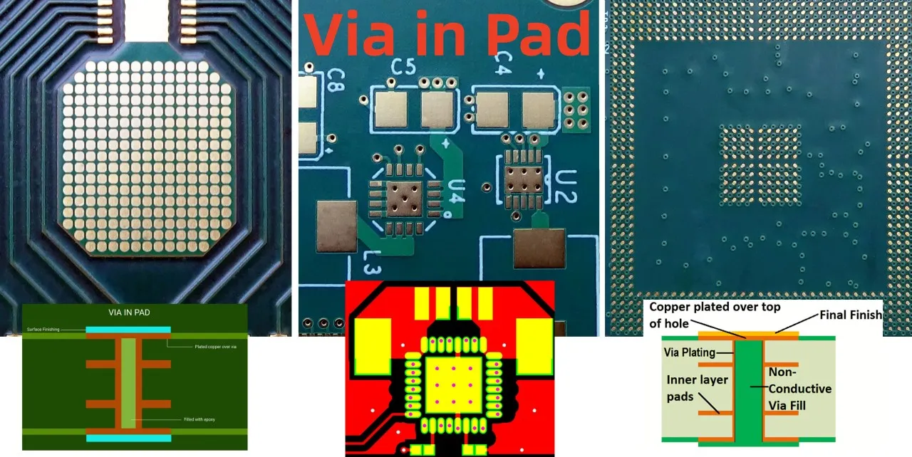
Via-in-Pad (VIP) is a PCB design technique where a via—a small hole that connects different layers of a circuit board—is placed directly inside the pad of a surface-mount component. Unlike traditional vias placed outside the pad, this method reduces the space needed for routing, making it ideal for high-density interconnect (HDI) designs. It is commonly used with fine-pitch components like Ball Grid Arrays (BGAs) and Quad Flat No-leads (QFNs), where space is extremely limited.
The primary benefit of VIP is its ability to maximize board density. By eliminating the need for additional routing space around pads, you can fit more components into a smaller area. Additionally, it enhances signal integrity by shortening trace lengths, which can reduce impedance mismatches and signal delays. For high-speed designs, this can mean the difference between a signal traveling at 5 GHz with minimal loss versus significant degradation over longer traces.
Via-in-Pad Design Guidelines for Optimal Results
Designing with Via-in-Pad requires careful planning to ensure manufacturability and performance. Below are key guidelines to follow when incorporating this technology into your high-density PCB layouts.
1. Via Size and Pad Compatibility
Ensure the via size matches the pad dimensions. A typical via diameter for VIP is between 0.2 mm and 0.3 mm for most HDI boards, with an annular ring (the copper surrounding the via) of at least 0.1 mm to maintain structural integrity. If the via is too large, it can weaken the pad and cause soldering issues. Check your design rules to confirm that the via fits within the pad without compromising the solder joint.
2. Use Filled or Plated-Over Vias
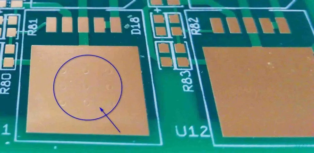
For VIP designs, vias are often filled with conductive or non-conductive material and then plated over (a process called Via-in-Pad Plated Over, or VIPPO). This prevents solder from wicking into the via during assembly, which could lead to weak joints or voids. Conductive fill materials also help with thermal dissipation, which we’ll discuss later.
3. Consider Component Pitch and Layer Count
For fine-pitch components like BGAs with a pitch of 0.5 mm or less, VIP is almost a necessity to route signals efficiently. Plan your layer stack-up carefully, as VIP often requires additional layers (e.g., 6 to 10 layers in HDI designs) to handle the increased routing density. Ensure your design software supports microvias if you’re working with extremely tight pitches.
4. Follow DFM Rules for Spacing
Maintain proper spacing between vias and other elements to avoid manufacturing defects. A minimum spacing of 0.2 mm between via edges is generally recommended, though this can vary based on your fabrication capabilities. Overcrowding can lead to issues like shorts or insufficient copper plating during manufacturing.
Via-in-Pad Manufacturing Process: What You Need to Know
The manufacturing process for Via-in-Pad designs is more complex than traditional PCB fabrication due to the need for precise via placement and filling. Understanding these steps can help you design boards that are easier to produce and less prone to defects.
1. Drilling and Plating
The process starts with drilling microvias directly into the pads using laser drilling for precision. These vias are then plated with copper to establish electrical connectivity between layers. The plating thickness should be at least 5 μm for standard designs and up to 12 μm for high-reliability applications to ensure durability.
2. Via Filling
After plating, the vias are filled with either conductive paste (like copper or silver epoxy) or non-conductive epoxy. Conductive fills improve thermal and electrical performance, while non-conductive fills are cheaper and prevent solder wicking. The choice depends on your design’s thermal and cost requirements.
3. Plating Over (VIPPO)
Once filled, the via is capped with a layer of copper through a process called plating over. This creates a flat surface on the pad, ensuring proper soldering during assembly. Without this step, solder can flow into the via, leading to uneven joints or component misalignment.
4. Surface Finish
The final step is applying a surface finish like ENIG (Electroless Nickel Immersion Gold) to protect the copper and ensure good solderability. This is especially important for VIP designs, as any surface irregularity can affect component placement.
Via-in-Pad Reliability: Ensuring Long-Term Performance
Reliability is a critical concern when using Via-in-Pad in high-density PCB designs. While VIP offers space-saving benefits, it can introduce risks if not implemented correctly. Here’s how to address potential reliability issues.
1. Solder Joint Integrity
Unfilled or improperly filled vias can lead to solder wicking, where solder flows into the via instead of forming a strong joint with the component. This can cause mechanical stress and eventual failure. Using filled and plated-over vias minimizes this risk, ensuring a reliable connection.
2. Mechanical Stress
Vias placed in pads are subject to mechanical stress during thermal cycling, especially in applications with temperature fluctuations (e.g., -40°C to 85°C). The difference in thermal expansion between the via fill material and the PCB substrate can cause cracks. Opt for conductive fills with thermal expansion properties similar to the board material to mitigate this issue.
3. Testing for Reliability
Perform thorough testing, such as thermal cycling tests and microsection analysis, to verify the integrity of VIP structures. For high-reliability applications like aerospace or medical devices, consider IPC Class 3 standards, which demand stricter manufacturing tolerances and testing protocols.
Thermal Management Via-in-Pad: Handling Heat in High-Density Designs
High-density PCBs often generate significant heat due to closely packed components and high-power signals. Via-in-Pad can play a crucial role in thermal management when designed with heat dissipation in mind.
1. Conductive Via Fills for Heat Dissipation
Using conductive materials like copper paste to fill vias enhances their ability to transfer heat away from components. For instance, in a design with a high-power QFN package dissipating 2-3 watts, VIP with conductive fill can reduce the junction temperature by up to 10°C compared to non-conductive fills.
2. Via Placement for Thermal Paths
Strategically place VIP structures under high-heat components to create direct thermal paths to inner copper layers or heat sinks. For example, placing multiple vias (e.g., 4-6) under a power IC can significantly improve heat distribution across the board.
3. Combine with Copper Pours
Connect VIP structures to large copper pours or planes on inner layers to spread heat more effectively. A copper plane with a thickness of 1 oz/ft2 can act as a heat sink, reducing thermal hotspots that might otherwise damage components.
Cost Analysis Via-in-Pad: Balancing Performance and Budget
While Via-in-Pad offers significant advantages for high-density PCB designs, it comes with added costs due to the complexity of manufacturing. Understanding these costs can help you make informed decisions for your projects.
1. Higher Fabrication Costs
The use of laser drilling, via filling, and plating-over processes increases fabrication costs compared to traditional via designs. For a typical HDI board, VIP can add 20-30% to the overall manufacturing cost, depending on the via count and fill material used.
2. Material Selection Impact
Conductive via fills, while better for thermal and electrical performance, are more expensive than non-conductive options. If thermal management isn’t a primary concern, opting for non-conductive epoxy can save up to 10-15% on material costs per board.
3. Yield and Defect Risks
VIP designs can lower manufacturing yield due to the precision required. Defects like incomplete via fills or plating issues can lead to rework or scrap, further driving up costs. Working with an experienced fabrication partner can minimize these risks, potentially saving 5-10% on defect-related losses.
4. Long-Term Savings
Despite higher upfront costs, VIP can reduce overall project expenses by enabling smaller board sizes and fewer layers in some designs. For high-volume production, a smaller board footprint can save thousands of dollars in material costs over time.
Best Practices for Implementing Via-in-Pad in Your Designs
To wrap up, here are some overarching best practices to ensure success with Via-in-Pad in your high-density PCB designs:
- Collaborate Early with Fabricators: Share your design files during the planning stage to confirm manufacturing capabilities and avoid costly redesigns.
- Use Simulation Tools: Leverage thermal and electrical simulation software to predict how VIP will impact heat dissipation and signal integrity.
- Start Small: If you’re new to VIP, test the technology on smaller, less critical projects before scaling to complex designs.
- Prioritize Reliability Testing: Invest in testing to catch potential issues early, especially for applications requiring long-term durability.
Conclusion: Unlocking the Full Potential of High-Density PCB Designs
Via-in-Pad technology is a game-changer for high-density PCB designs, offering unmatched space savings and performance benefits. By following proper design guidelines, understanding the manufacturing process, addressing reliability concerns, optimizing thermal management, and carefully analyzing costs, you can harness the full potential of VIP in your projects. This approach not only maximizes board density but also ensures your designs meet the demands of modern electronics, from consumer gadgets to industrial systems.
At ALLPCB, we’re committed to supporting engineers with the tools and expertise needed to bring innovative designs to life. With a focus on quality and precision, we’re here to help you navigate the complexities of Via-in-Pad and other advanced PCB technologies. Start integrating these strategies into your next project and see the difference in performance and efficiency.


