ALLPCB


If you're new to PCB design and wondering how to avoid expensive errors, you've come to the right place. PCB manufacturability checks are essential steps to ensure your design can be produced without issues, saving you time and money. In this beginner's guide, we'll walk you through the key checks for PCB design, common manufacturability issues, and practical tips for creating simple PCB designs, including DIY methods like home etching and the toner transfer method.
Whether you're a hobbyist experimenting with DIY PCB projects or an aspiring engineer tackling your first professional board, understanding manufacturability is crucial. Let's dive into the details of how to design with production in mind and avoid costly mistakes.
Why PCB Manufacturability Matters for Beginners
Designing a printed circuit board (PCB) is exciting, but if your design isn't manufacturable, it can lead to delays, wasted materials, and unexpected costs. Manufacturability refers to how easily and accurately a PCB design can be turned into a physical board. For beginners, overlooking this aspect often results in boards that can't be fabricated or don't work as intended.
By performing manufacturability checks early in the design process, you can catch potential issues before they become expensive problems. These checks ensure that your design meets the capabilities of manufacturing equipment and adheres to industry standards. This is especially important for DIY enthusiasts using home etching or toner transfer methods, where precision and simplicity are key.
Key Manufacturability Checks for PCB Design Beginners
Before sending your design for production or starting a DIY project, run through these essential manufacturability checks. They will help you spot errors and ensure your PCB can be made without hiccups.
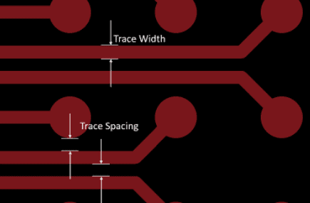
1. Check Minimum Trace Width and Spacing
Every manufacturing process has limits on how thin traces (the copper lines on your PCB) can be and how close they can be to each other. For most standard processes, the minimum trace width and spacing are around 6 mils (0.006 inches). If your traces are too thin or too close, they might break during fabrication or cause short circuits.
For beginners, aim for wider traces and spacing, such as 10 mils or more, to stay on the safe side. This is especially important in DIY PCB projects using home etching, where precision is harder to achieve compared to professional equipment.
Tip: Use design software with built-in design rule checks (DRC) to automatically flag traces or spacing that fall below the minimum limits.
2. Verify Drill Hole Sizes
Drill holes are used for mounting components and creating vias (connections between layers). Each manufacturer or DIY etching setup has a minimum and maximum drill size. Typically, the smallest drill size for standard fabrication is around 0.3 mm (12 mils). If your holes are too small, they might not be drilled accurately, leading to broken connections.
For DIY PCB at home, ensure your drill bits match the hole sizes in your design. Using a toner transfer method, double-check that the printed design transfers accurately to avoid misaligned holes.
Tip: Stick to standard hole sizes like 0.8 mm or 1 mm for through-hole components to avoid issues.
3. Ensure Proper Component Placement
Placing components too close to each other or to the board's edge can cause assembly problems. For manufacturability, maintain a clearance of at least 0.1 inches (2.54 mm) between components and from the board edge. This gives enough room for soldering and prevents damage during cutting or handling.
In DIY PCB projects, overcrowding can also make hand-soldering difficult. Leave extra space to make your work easier, especially if you're new to soldering.

4. Check Copper Pour and Ground Planes
Copper pours and ground planes help reduce noise and improve signal integrity, but they must be designed carefully. Avoid isolated copper areas (also called "dead copper") that aren't connected to any net, as they can act as antennas and cause interference. For beginners, ensure all copper areas are tied to a ground or power net.
In terms of signal integrity, poorly designed ground planes can lead to issues like crosstalk or electromagnetic interference (EMI). Keep high-speed signals (above 50 MHz) away from edges of ground planes to minimize signal reflection.
5. Review Solder Mask and Silkscreen
The solder mask is the protective layer over the copper traces, and the silkscreen is the printed text or symbols on the board. Ensure the solder mask openings are slightly larger than the pads (typically by 4 mils or 0.1 mm) to prevent soldering issues. For silkscreen, avoid placing text over pads or vias, as it can interfere with assembly.
For DIY PCB using toner transfer, you won't have a professional solder mask, so be extra careful during soldering to avoid shorts. You can apply a DIY protective layer like nail polish over traces after etching.
Common Manufacturability Issues in PCB Design for Beginners
Even with careful planning, beginners often encounter manufacturability issues. Here are some frequent mistakes and how to avoid them.
1. Ignoring Manufacturer Guidelines
Every fabrication house has specific design rules, such as minimum trace widths, hole sizes, and layer stack-up requirements. Failing to follow these can result in a design that can't be produced. For professional projects, always download and review the design guidelines before starting.
For DIY PCB at home, your limitations will depend on your tools and methods. For instance, with home etching using ferric chloride, achieving traces thinner than 10 mils can be challenging due to under-etching or over-etching.
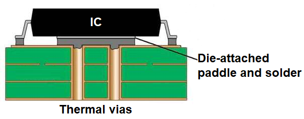
2. Overlooking Thermal Management
Components like power regulators or high-current ICs generate heat, and without proper thermal design, your PCB can fail. Beginners often forget to add thermal vias or sufficient copper area for heat dissipation. As a rule of thumb, place thermal vias (0.3 mm diameter, spaced 1 mm apart) under high-heat components to transfer heat to the opposite side of the board.
In DIY designs, where multi-layer boards aren't an option, use larger copper areas around heat-generating parts to help spread the heat.
3. Poor Signal Integrity Planning
For designs with high-speed signals (like USB or HDMI, operating at 480 Mbps or higher), signal integrity is critical. Beginners often route traces haphazardly, leading to signal loss or interference. Keep high-speed traces short and direct, avoid sharp 90-degree bends, and maintain consistent impedance (typically 50 ohms for single-ended signals).
For simple PCB design projects, if you're not dealing with high-speed signals, this may not be a concern. Focus on clean, organized routing instead.
Simple PCB Design Tips for Beginners
Creating a manufacturable PCB doesn't have to be complicated. Follow these tips to keep your design simple and effective, whether you're aiming for professional production or a DIY project.
1. Start with a Schematic
Always begin with a clear schematic before moving to layout. A schematic is like a blueprint for your circuit, showing how components connect. This step helps you avoid wiring mistakes in the layout phase. Most design software allows you to convert your schematic directly into a PCB layout, making the process smoother.
2. Use a Grid for Layout
Align components and traces to a grid (like 0.1 inch or 2.54 mm spacing) to keep your design neat. A grid makes routing easier and ensures consistent spacing, which is vital for manufacturability. This is especially helpful in DIY PCB projects, where manual alignment can be tricky.
3. Test Small Designs First
If you're new to PCB design, start with small, simple boards before tackling complex projects. A basic LED circuit or a single transistor amplifier is a great starting point. Testing small designs helps you learn the process and catch mistakes without wasting resources.
DIY PCB: Home Etching and Toner Transfer Method
For hobbyists and beginners, creating a PCB at home using DIY methods like home etching and the toner transfer method is a cost-effective way to experiment. Here's how to ensure manufacturability with these techniques.
1. Understanding Home Etching
Home etching involves using a chemical solution (like ferric chloride) to remove unwanted copper from a blank PCB, leaving only your designed traces. To ensure manufacturability:
- Use a copper-clad board with a thickness of 1.6 mm for durability.
- Keep trace widths above 10 mils, as finer traces may dissolve during etching.
- Work in a well-ventilated area and wear protective gear, as etching chemicals are hazardous.
2. Mastering the Toner Transfer Method
The toner transfer method uses a laser printer to print your PCB design onto special paper, which is then transferred to the copper board using heat (like an iron). For best results:
- Print your design in mirror mode so it transfers correctly.
- Use high heat and firm pressure with the iron for 2-3 minutes to ensure the toner sticks to the copper.
- After cooling, soak the board in water to remove the paper, leaving the toner as an etch-resistant mask.
This method works well for simple PCB designs but struggles with fine details below 8 mils. Test your design on a small scale first to confirm the transfer quality.

How to Avoid Costly Mistakes in PCB Design
Mistakes in PCB design can lead to boards that don't work or can't be made. Here are actionable ways to prevent costly errors as a beginner.
1. Run Design Rule Checks (DRC)
Most design software includes a DRC feature that automatically checks for issues like trace spacing, hole sizes, and clearance violations. Run a DRC before finalizing your design to catch errors early. For DIY projects, manually double-check your layout against your chosen manufacturing limits.
2. Prototype Before Mass Production
Even with thorough checks, small issues can slip through. Create a prototype of your PCB to test functionality before ordering a large batch. For DIY enthusiasts, etch a single board at home to verify your design works as expected.
3. Keep Documentation Clear
Maintain detailed notes on your design, including component values, trace widths, and layer information. Clear documentation helps during troubleshooting and ensures you can replicate or modify the design later. For professional fabrication, include a Bill of Materials (BOM) and assembly drawings.
Conclusion: Master PCB Manufacturability with Practice
Designing a PCB as a beginner can feel overwhelming, but with the right manufacturability checks, you can avoid costly mistakes and create boards that work as intended. Focus on basics like trace width, spacing, and component placement, and always review your design against manufacturing guidelines—whether you're sending it for professional production or crafting a DIY PCB at home with etching or toner transfer methods.
Start small, test often, and learn from each project. With practice, you'll gain confidence in creating simple PCB designs that are both functional and manufacturable. By prioritizing these steps, you're setting yourself up for success in every PCB project, no matter the complexity.