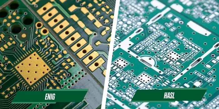
Advanced Mobile Phone PCB Stackup Designs for High Speed Data
Explore advanced mobile phone PCB stackup designs for high-speed data, covering controlled impedance, microstrip, stripline, and layer spacing.
Explore how standard PCB dimensions affect signal integrity, with tips on impedance control and high-speed design for optimal performance.
Learn to build a PCB for ultrasonic gesture recognition. Create touchless control systems with our guide on gesture sensor PCB design.
Learn strategies for minimizing crosstalk in 4-layer PCBs with tips on trace spacing, guard traces, and signal isolation techniques.
Explore thermal management for wearable health monitor PCBs with strategies like thermal vias, cooling techniques, and simulation for optimal design.
Learn multi-layer PCB design for beginners with this guide on easy first projects, simple layouts, and DIY electronics tips from ALLPCB.
Explore advanced 16-layer PCB stackup design for optimal signal integrity and impedance control with practical tips from ALLPCB.
Explore PCB impedance in high-speed design, covering testing, control, TDR, VNA, and signal integrity for reliable electronics performance.
Explore signal skew in high-speed military radar PCBs, with tips on differential pair routing, trace matching, and managing propagation delay.
Explore military radar PCB design for extreme temperatures, focusing on high-temperature materials, thermal stress, and CTE mismatch solutions.
Explore how AI optimizes wearable health monitor PCB design with automated layout, machine learning, and smart PCB tech for better efficiency.
Explore signal integrity in security camera PCBs for high-quality video. Learn layout tips, impedance control, and noise reduction techniques.
Learn PCB design for EMC with diagnostic tools like near field scanning and spectrum analyzers, plus tips on grounding and EMI shielding.
Explore the role of copper weight in 4-layer PCBs, balancing current capacity and signal integrity for optimal design and performance.
Explore the importance of controlled impedance in military radar PCB design, covering impedance matching, TDR testing, and signal integrity.
Explore how V-scoring impacts PCB signal integrity, impedance, and design. Learn tips to optimize your PCB for performance and reliability.
Explore how copper weight impacts trace-to-pad spacing in PCB design, affecting trace width, current capacity, voltage drop, and thermal management.
Explore the science of gold plating, from chemistry and physics to soft gold electroplating principles and surface finishing metallurgy.
Learn the dos and don'ts of V-Scoring your PCB. Get tips on what to do, what to avoid, and the correct way to use V-Scoring for success.
Learn about via-to-via spacing in different potentials for PCB design. Discover key factors, tips, and standards for safe, reliable layouts.