


In the intricate world of electronics, the printed circuit boards (PCBs) is evolving at a rapid pace. One of the most advanced types of PCBs is the 8-layer PCB, a marvel of modern engineering designed to meet the demands of high-performance and compact electronic devices. This blog post will guide you through the intricacies of 8-layer PCBs, shedding light on when and why they are used, the design considerations involved, their manufacturing process, and their applications. By the end of this article, you'll have a comprehensive understanding of 8-layer PCBs and how they can revolutionize your electronic projects.
What is 8 Layer PCB?
An 8-layer PCB is a type of multilayer PCB that consists of eight alternating layers of conductive copper and insulating material. This intricate stackup allows for greater functionality and complexity in electronic circuits. Each layer serves a specific purpose, whether it's for signal routing, power distribution, or ground planes, contributing to the overall performance and reliability of the electronic device.
When and Why to Use 8-Layer PCBs
High-Density Interconnect (HDI) Applications
8-layer HDI PCBs are particularly useful in high-density interconnect (HDI) applications. When electronic devices require complex circuitry within a limited space, 8-layer PCBs offer the ideal solution. Their multiple layers allow for increased routing options, reducing the need for long and convoluted traces.
Enhanced Signal Integrity
Signal integrity is a critical factor in high-speed electronic circuits. The additional layers in an 8-layer PCB help in separating signal layers with ground or power planes, minimizing crosstalk and electromagnetic interference (EMI). This results in more reliable signal transmission.
Efficient Power Distribution
For devices that consume significant power, managing power distribution efficiently is crucial. 8-layer PCBs provide additional layers for power planes, ensuring stable and efficient power delivery to various components.
Design of 8-Layer PCBs
Layer Stackup Configuration
Designing an 8-layer PCB requires careful consideration of the layer stackup configuration. A typical 8-layer PCB might include layers designated for signals, ground planes, and power planes. Proper arrangement of these layers is essential to optimize performance and minimize EMI.
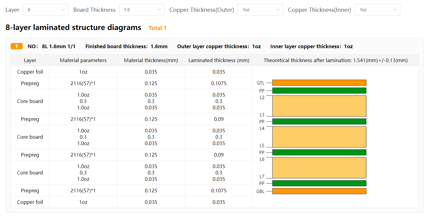
ALLPCB can recommend stackup structures according to the Board Thickness,
Inner Copper Thickness, and Outer Copper Thickness. You can check our 8-layer-laminated structure diagrams.
Routing Direction
In an 8-layer PCB, adjacent signal layers should be routed perpendicularly to each other to minimize crosstalk. This routing strategy helps in maintaining signal integrity, especially in high-speed circuits.
Return Path Management
High-speed signals require a clear and short return path to minimize interference. Ensuring that the return path does not overlap with other signal paths is crucial for maintaining signal integrity.
Ground Plane Considerations
A continuous ground plane is essential for reducing impedance discontinuities and providing a stable reference for signal layers. Splitting the ground plane can lead to performance issues, so it's best to keep it intact.
Suggested Reading: www.allpcb.com/blog/pcb-knowledge/8-layer-pcb-art-designing-functional-and-beautiful-circuit-boards.html
Manufacturing of 8-Layer PCBs
Material Selection
The choice of materials for the different layers in an 8-layer PCB significantly impacts its performance. Common materials include PCB material FR4 for the core and prepregs, but high-speed materials like Rogers or Isola may be used for specific applications requiring better signal integrity.
Layer Alignment and Bonding
During manufacturing, precise alignment of the layers is critical to ensure the functionality of the PCB. The layers are bonded together using heat and pressure, creating a unified structure.
Etching and Plating
The conductive layers are etched to create the desired circuit patterns, and holes are drilled and plated to create vias that connect the different layers. These processes require high precision to maintain the integrity of the design.
Quality Control and Testing
Rigorous quality control measures are employed to ensure the reliability of 8-layer PCBs. These include visual inspections, electrical testing, and thermal analysis to detect any defects or performance issues.
Applications of 8-Layer PCBs
Telecommunications
In telecommunications equipment, 8-layer PCBs are used to manage complex signal routing and power distribution, ensuring reliable communication.
Aerospace and Defense
Aerospace and defense systems require high-performance, reliable PCBs. 8-layer PCBs provide the necessary complexity and robustness to meet these demands.
Consumer Electronics
From smartphones to gaming consoles, consumer electronics benefit from the compact and efficient design of 8-layer PCBs, which enable advanced features and functionality.
Automotive Industry
In modern vehicles, electronic systems control everything from infotainment to advanced driver-assistance systems (ADAS). 8-layer PCBs are integral in managing these complex electronic circuits.
Challenges in Designing 8-Layer PCBs
Cost Considerations
The complexity of 8-layer PCBs makes them more expensive to design and manufacture compared to simpler PCBs. However, the performance benefits often justify the higher cost.
Material Compatibility
Ensuring compatibility between different materials used in the PCB stackup is crucial for reliable performance. Incompatible materials can lead to issues like signal distortion or mechanical failure.
Manufacturing Limitations
Not all manufacturers have the capability to produce high-quality 8-layer PCBs. It's important to choose a manufacturer with expertise in multilayer PCB fabrication.
Conclusion
The 8-layer PCB is a testament to the advancements in PCB design and manufacturing. Its ability to handle complex circuits, enhance signal integrity, and efficiently distribute power makes it an indispensable component in modern electronic devices. Whether you're an electronic engineer, PCB designer, or tech startup, understanding the intricacies of 8-layer PCBs can significantly enhance your projects. For further assistance and expert guidance, consider signing up with ALLPCB for free to explore more about PCB design and manufacturing best practices. The future of electronics is layered, and mastering 8-layer PCBs is your key to staying ahead in this rapidly evolving field.