 ALLPCB


If you're a hobbyist or student looking to create custom circuit boards for simple lab devices, DIY PCB etching is an accessible and rewarding skill to learn. This guide will walk you through the entire process of DIY PCB etching for hobbyists, from designing your board to using safe chemicals at home. Whether you're searching for a PCB etching tutorial for beginners or ideas for simple PCB projects for students, this step-by-step resource will help you set up a homemade PCB fabrication lab and master the basics of PCB creation.
In the sections below, we'll cover everything you need to know, including a detailed PCB etching chemicals guide, safety tips, and practical advice for crafting functional boards for small projects. Let's dive in and start building!
What is PCB Etching and Why Do It Yourself?
PCB etching is the process of removing unwanted copper from a copper-clad board to create conductive traces that form the circuits of your electronic device. These traces connect components like resistors, capacitors, and microcontrollers, turning a blank board into a functional printed circuit board (PCB).
For hobbyists and students, DIY PCB etching offers several benefits. It’s cost-effective compared to ordering professionally manufactured boards, especially for small or one-off projects. It also gives you full control over the design and allows for quick prototyping in your own homemade PCB fabrication lab. Plus, the hands-on experience is a fantastic way to learn about electronics and circuit design.
Getting Started: Tools and Materials for DIY PCB Etching
Before you begin, gather the necessary tools and materials. Most of these items are affordable and easy to find at hardware stores or online. Here’s a comprehensive list to set up your workspace for DIY PCB etching for hobbyists:
- Copper-Clad Board: This is the base material for your PCB, typically made of fiberglass (FR-4) with a thin layer of copper on one or both sides. A single-sided board (1.6mm thickness) is ideal for beginners.
- Design Software: Use free software to create your PCB layout. Popular options include tools that allow you to draw schematics and convert them into board layouts.
- Laser Printer or Marker Pen: For transferring your design onto the board. A laser printer works best for precision, but a permanent marker can suffice for very simple designs.
- Etching Chemicals: Common options include ferric chloride or a homemade mix of vinegar and hydrogen peroxide (detailed in the PCB etching chemicals guide section below).
- Protective Gear: Safety goggles, gloves, and a well-ventilated workspace are essential when handling chemicals.
- Drill or Drill Bits: For creating holes to mount components (a small hand drill or a 0.8-1.2mm bit works well).
- Plastic Containers: Non-metallic trays or bowls for holding the etching solution.
- Sandpaper or Steel Wool: To clean the copper surface before etching.
- Acetone or Rubbing Alcohol: For cleaning the board after etching.
Step-by-Step PCB Etching Tutorial for Beginners
Now that you have your tools ready, let’s walk through the process of creating a PCB for a simple lab device, like a basic LED circuit or a small sensor module. This PCB etching tutorial for beginners breaks down each step clearly.
Step 1: Design Your Circuit
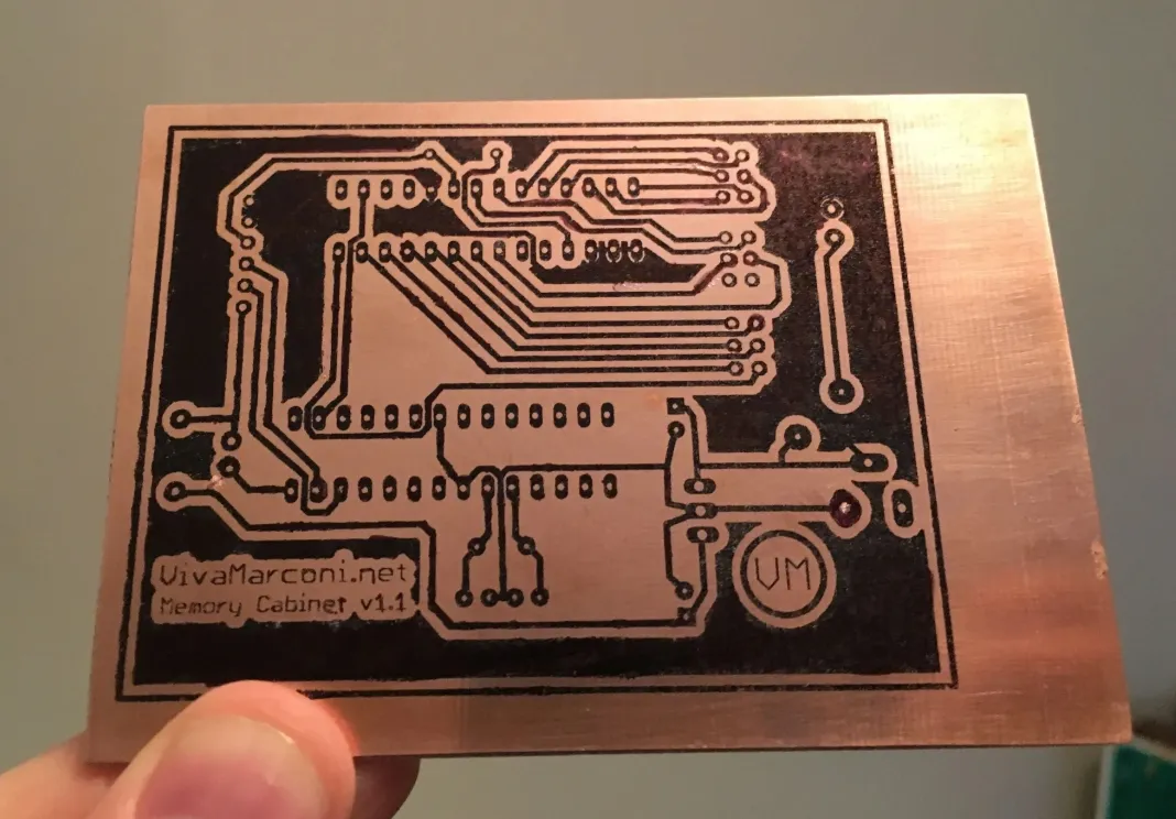
Start by designing your circuit using PCB design software. For beginners, focus on simple PCB projects for students, such as a circuit to power a few LEDs or a basic timer using a 555 IC chip. Ensure your design accounts for trace width (typically 0.3-0.5mm for low-current applications) and spacing to avoid short circuits. Once your design is ready, print it on glossy paper using a laser printer, ensuring the traces are black and opaque. This printout will act as a mask for transferring the design to the board.
Step 2: Prepare the Copper-Clad Board
Cut the copper-clad board to the size of your design using a hacksaw or utility knife. Clean the copper surface with fine sandpaper or steel wool to remove oxidation and ensure a smooth, shiny finish. A clean surface helps the design transfer properly and ensures even etching.
Step 3: Transfer the Design to the Board
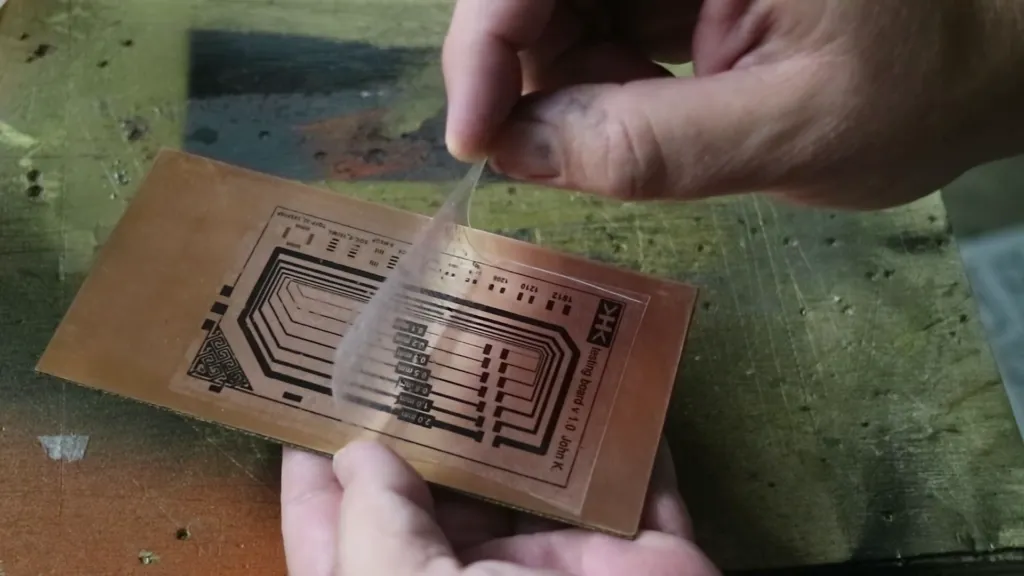
Place the printed design face-down on the copper side of the board. Use a hot iron (set to medium heat, around 150-200°C) to transfer the toner from the paper to the copper. Press firmly for 2-3 minutes, ensuring even heat distribution. After cooling, soak the board in water to peel off the paper, leaving the toner traces on the copper. If any lines are incomplete, use a permanent marker to touch them up.
Step 4: Etch the Board
Place the board in a plastic container and pour in your etching solution (see the PCB etching chemicals guide below for options). The solution will dissolve the exposed copper, leaving only the areas protected by the toner. This process can take 10-30 minutes depending on the chemical used and the copper thickness (typically 1 oz/ft2 or 35 μm). Gently agitate the container to speed up the process and ensure even etching. Once the unprotected copper is gone, remove the board and rinse it thoroughly with water.
Step 5: Clean and Drill the Board
Use acetone or rubbing alcohol to remove the toner, revealing the copper traces underneath. Inspect the traces for any breaks or defects. Then, drill holes at the designated spots for component leads using a small drill bit (0.8mm is common for most through-hole components). Sand the edges of the board if needed for a clean finish.
Step 6: Test and Assemble
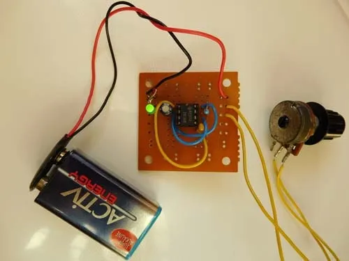
Check the continuity of the traces using a multimeter to ensure there are no breaks or shorts. If everything looks good, solder your components onto the board. For a simple lab device, ensure proper polarity for components like LEDs (forward voltage typically around 2-3V for standard LEDs) and capacitors.
PCB Etching Chemicals Guide: Safe Options for Home Use
Choosing the right etching solution is crucial for safety and effectiveness. This PCB etching chemicals guide outlines two common options for hobbyists working in a homemade PCB fabrication lab.
Ferric Chloride
Ferric chloride is a traditional etching chemical widely used for PCB fabrication. It’s effective and relatively fast, etching a standard 1 oz/ft2 copper board in about 10-15 minutes at room temperature (20-25°C). However, it’s corrosive and can stain surfaces, so handle it with care. Always wear gloves and goggles, and work in a well-ventilated area. Dispose of used ferric chloride responsibly, as it’s hazardous to the environment—check local regulations for proper disposal methods.
Vinegar and Hydrogen Peroxide Mix
For a safer, more accessible alternative, you can create an etching solution using household items: white vinegar, hydrogen peroxide (3% concentration), and table salt. Mix equal parts vinegar and hydrogen peroxide (e.g., 100ml each), then add a teaspoon of salt to accelerate the reaction. This solution is slower than ferric chloride, often taking 30-60 minutes to etch, but it’s less toxic and easier to handle. Still, use protective gear and ventilate your workspace, as the reaction produces small amounts of gas.
Simple PCB Projects for Students to Practice Etching
If you’re new to PCB etching, start with simple PCB projects for students to build confidence. Here are three beginner-friendly ideas for lab devices that use minimal components and basic circuits:
1. LED Blinking Circuit
Create a circuit that blinks an LED using a 555 timer IC. This project introduces you to timing components and requires only a few resistors (e.g., 1kΩ and 10kΩ) and capacitors (e.g., 10μF). The blinking rate can be adjusted by changing the resistor values, with a typical frequency of 1-2 Hz for visible blinking.
2. Basic Voltage Regulator
Design a PCB for a simple voltage regulator using a 7805 IC to output a stable 5V from a higher input (e.g., 9V battery). This is useful for powering small lab devices and teaches you about power supply design. Include capacitors (0.1μF and 1μF) on the input and output for stability.
3. Light Sensor Module
Build a circuit that turns on an LED when it gets dark using a light-dependent resistor (LDR) and a transistor (e.g., BC547). This project is great for learning about sensors and requires traces with low current capacity (typically under 20mA for the LED).
Safety Tips for DIY PCB Etching at Home
Working with chemicals and tools in your homemade PCB fabrication lab requires caution. Follow these safety tips to protect yourself and your workspace:
- Always wear safety goggles and chemical-resistant gloves when handling etching solutions.
- Work in a well-ventilated area to avoid inhaling fumes from chemicals like ferric chloride or peroxide mixes.
- Keep etching solutions away from skin and eyes. If contact occurs, rinse immediately with plenty of water.
- Store chemicals in labeled, sealed containers out of reach of children or pets.
- Use plastic or glass containers for etching—never metal, as it can react with the chemicals.
- Dispose of used chemicals properly. Do not pour them down the drain; check local guidelines for hazardous waste disposal.
Troubleshooting Common Issues in PCB Etching
Even with careful planning, issues can arise during DIY PCB etching for hobbyists. Here are solutions to common problems:
- Uneven Etching: If some copper remains after etching, ensure the solution is agitated evenly during the process. Increase etching time slightly or raise the solution temperature to 30-40°C for faster reaction.
- Broken Traces: If toner doesn’t transfer properly, causing broken traces, double-check your ironing technique or use a higher heat setting. Touch up gaps with a marker before etching.
- Over-Etching: If traces are too thin or disappear, reduce etching time or dilute the solution slightly. Check the board frequently during etching.
Scaling Up: Advancing Your Homemade PCB Fabrication Lab
Once you’re comfortable with basic etching, consider upgrading your homemade PCB fabrication lab for more complex projects. Invest in a small CNC drill for precise hole placement or experiment with double-sided boards for denser circuits. You can also explore photoresist methods for finer traces (down to 0.2mm width), which involve UV exposure and developer solutions for professional-quality results.
Conclusion: Start Etching Today!
DIY PCB etching is a fantastic way for hobbyists and students to bring their electronic ideas to life. With this PCB etching tutorial for beginners, you now have the knowledge to create custom boards for simple PCB projects for students right in your own homemade PCB fabrication lab. From understanding the process to following our PCB etching chemicals guide, you’re ready to tackle DIY PCB etching for hobbyists with confidence.
Grab your materials, set up a safe workspace, and start experimenting with small lab devices. Each project will build your skills and open up new possibilities in electronics design. Happy etching!


