ALLPCB


In the world of electronics, printed circuit boards (PCBs) are the backbone of functionality. But what if they could be more than just technical components? With 8-layer PCB art, you can create designs that are both functional and visually stunning. Let's be with ALLPCB to dive into the exciting realm of PCB art design, exploring creative PCB layouts, artistic PCB projects, and how to use a PCB as a canvas while maintaining its core functionality. Whether you're an engineer, designer, or hobbyist, you'll find practical tips and inspiration to elevate your next project with functional PCB art.
What Is 8-Layer PCB Art?
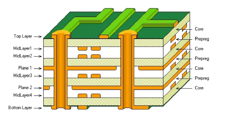
At its core, 8-layer PCB art is the fusion of technical design and aesthetic creativity on a multi-layered circuit board. An 8 layer PCB consists of eight conductive layers separated by insulating materials, often used in complex electronics like high-speed communication devices or advanced computing systems. By leveraging these layers, designers can craft intricate patterns, images, or textures on the board's surface or within its internal layers, turning a functional piece into a work of art.
Unlike the single or double layer PCB, an 8-layer PCB offers more space for creative PCB layouts. You can dedicate specific layers to artistic elements while reserving others for critical electrical routing. This balance ensures that the board remains fully functional while showcasing stunning visual designs. Think of it as turning a PCB into a canvas where every trace, via, and silkscreen contributes to both form and function.
Why Choose an 8-Layer PCB for Artistic Projects?
Creating artistic PCB projects with an 8-layer board offers unique advantages over simpler designs. Here’s why this approach stands out for functional PCB art:
- More Design Space: With eight layers, you have additional room to separate artistic elements from critical circuitry. For instance, you can use the top and bottom layers for visual designs while routing high-speed signals (up to 10 Gbps in some cases) on internal layers to avoid interference.
- Enhanced Functionality: The complexity of an 8-layer PCB supports advanced projects with tight impedance control (often targeting 50 ohms for high-frequency signals), making it ideal for both art and performance.
- Visual Depth: By incorporating designs across multiple layers, you can create a sense of depth or hidden patterns that become visible under specific lighting or angles, adding a unique flair to your PCB as a canvas.
These benefits make 8-layer PCBs a perfect choice for designers looking to push the boundaries of creativity without sacrificing functionality.
Steps to Design Functional and Beautiful 8-Layer PCB Art
Designing an 8-layer PCB that balances art and function requires careful planning. Below are actionable steps to guide you through the process of creating creative PCB layouts and artistic PCB projects.
1. Define Your Artistic Vision
Start by deciding what kind of visual impact you want your PCB to have. Are you aiming for a minimalist pattern, a detailed image, or a thematic design like a circuit board inspired by nature? Keep in mind that your PCB art design should complement its purpose. For example, if the board is for a gaming device, you might incorporate pixelated graphics or joystick silhouettes into the silkscreen layer.
Remember to consider how the artistic elements will fit within the constraints of an 8-layer structure. Plan which layers will hold the artwork and which will focus on electrical routing to avoid signal interference.
2. Choose the Right Tools for PCB Art Design
To bring your vision to life, you'll need design software that supports multi-layer PCB layouts and allows for creative freedom. Many popular tools offer features to import images or draw custom shapes directly onto the board. Look for software with robust layer management to assign specific layers for art while keeping others dedicated to functionality.
For artistic elements, focus on the silkscreen layer (used for text and symbols) and copper layers for conductive patterns that double as art. Ensure the software supports high-resolution imports if you're converting an image into a PCB trace or silkscreen design.
3. Plan Layer Usage for Art and Function
In an 8-layer PCB, each layer serves a purpose. Here’s a typical breakdown to balance creative PCB layouts with functionality:
- Top and Bottom Layers: Use for silkscreen art or simple copper patterns visible on the surface. These layers are perfect for bold designs or logos.
- Internal Layers 2-7: Reserve for critical signal routing and power/ground planes. For high-speed designs, maintain controlled impedance (e.g., 50 ohms for differential pairs) on these layers.
- Hidden Art: If your design allows, etch subtle patterns on internal copper layers. Though not visible in the final product, these can be a creative touch for transparent or cutaway boards.
By separating art from critical components, you ensure the board remains functional while showcasing your artistic PCB project.
4. Incorporate Artistic Elements Without Compromising Performance
One of the biggest challenges in functional PCB art is ensuring that artistic additions don’t interfere with electrical performance. Here are some tips to maintain balance:
- Avoid Critical Areas: Keep artistic traces or silkscreen designs away from high-speed signal paths or areas with strict impedance requirements (e.g., 50 ohms for USB 3.0 signals).
- Use Silkscreen Wisely: The silkscreen layer is non-conductive, so it’s a safe space for detailed artwork like text, icons, or patterns without affecting functionality.
- Test for Interference: Simulate your design to check for electromagnetic interference (EMI) caused by large copper art pieces. Adjust the layout if necessary to minimize noise.
5. Select Materials and Finishes for Visual Impact
The materials and finishes you choose for your 8-layer PCB can enhance its artistic appeal. Consider the following options:
- Solder Mask Colors: Go beyond standard green with colors like black, white, red, or blue to make your PCB art design pop. A matte black finish can create a sleek, modern look for intricate silkscreen patterns.
- Surface Finishes: Options like ENIG (Electroless Nickel Immersion Gold) provide a shiny gold finish that contrasts beautifully with darker solder masks, highlighting copper art.
- Transparency: For a unique effect, consider using transparent substrates in certain areas to reveal internal layer art, adding depth to your PCB as a canvas.
These choices not only improve aesthetics but also protect the board, ensuring it remains functional in real-world applications.
6. Prototype and Iterate
Before finalizing your design, create a prototype to test both the functionality and visual impact of your artistic PCB project. Check for issues like signal integrity (ensuring minimal crosstalk at high frequencies, such as 5 GHz for wireless applications) and verify that the artwork aligns with your vision. Use feedback from testing to refine the design, adjusting artistic elements or routing as needed.
Suggested Reading: Prototyping 8-Layer PCBs: Fast Turnaround and Design Validation
Inspiration for Creative PCB Layouts
Need ideas for your next 8-layer PCB art project? Here are a few creative concepts to spark inspiration:
- Nature-Inspired Designs: Etch leaf patterns or waveforms into the top copper layer to evoke natural beauty, perfect for environmental tech projects.
- Geometric Patterns: Use repeating shapes like hexagons or fractals on the silkscreen for a modern, tech-savvy look that complements high-performance boards.
- Storytelling Through Layers: Create a narrative by designing different elements on each layer, visible through cutouts or transparency, turning your PCB into a multi-dimensional canvas.
Challenges in 8-Layer PCB Art and How to Overcome Them
While designing functional PCB art on an 8-layer board is rewarding, it comes with challenges. Here’s how to address common issues:
- Balancing Art and Function: As mentioned earlier, separate artistic elements from critical routing. Use simulation tools to ensure artwork doesn’t disrupt signal integrity (e.g., maintaining a 100-ohm differential impedance for Ethernet signals).
- Manufacturing Constraints: Complex designs may increase production costs or face limitations in etching precision. Work closely with your manufacturing partner to understand their capabilities and adjust your design accordingly.
- Time Investment: Crafting detailed PCB art takes time. Plan your project timeline to account for multiple iterations and testing phases to perfect both aesthetics and performance.
Applications of 8-Layer PCB Art
Functional PCB art isn’t just for show—it has real-world applications across various industries. Here are a few examples:
- Consumer Electronics: Add branded designs or unique patterns to device motherboards, making them visually appealing during repairs or showcases.
- Art Installations: Use 8-layer PCBs in interactive art pieces where the board itself is part of the exhibit, blending technology with creativity.
- Educational Tools: Design visually engaging circuit boards for teaching electronics, helping students connect with the material through art.
Tips for Beginners in PCB Art Design
If you’re new to creating artistic PCB projects, start with these beginner-friendly tips:
- Start Simple: Begin with basic silkscreen designs before experimenting with copper layer art or multi-layer effects.
- Learn from Others: Study existing PCB art designs online for inspiration and to understand how artists balance form and function.
- Focus on Functionality First: Ensure your board works perfectly before adding artistic elements. A beautiful design is useless if the circuit fails.
Conclusion
8-layer PCB art opens up a world of possibilities for designers and engineers who want to combine creativity with cutting-edge technology. By treating a PCB as a canvas, you can craft creative PCB layouts and artistic PCB projects that are both functional and beautiful. From planning your design across multiple layers to choosing the right materials for visual impact, every step offers a chance to innovate. With careful attention to detail and a balance of art and engineering, your 8-layer PCB can become a masterpiece that stands out in both performance and aesthetics.
Whether you’re working on a personal project or a professional product, functional PCB art allows you to push boundaries and make a lasting impression. Dive into the world of PCB art design today and transform your circuit boards into something extraordinary.