 ALLPCB


If you're an engineer looking to streamline PCB production, understanding PCB panelization and V-scoring is key to achieving efficient manufacturing and cost savings. In this guide, we’ll dive deep into how V-scoring enhances V-scoring panel layout, improves V-scoring manufacturability, and aligns with V-scoring design for manufacturing (DFM) principles. Whether you're designing a single board or preparing for mass production, this blog will equip you with actionable insights to optimize your process.
What is PCB Panelization and Why Does It Matter?
PCB panelization is the process of grouping multiple printed circuit boards (PCBs) onto a single larger panel for manufacturing. This technique boosts efficiency by allowing manufacturers to process several boards at once, reducing material waste and cutting production costs. For engineers, panelization is a critical step in ensuring that designs transition smoothly from prototype to production.
The benefits of panelization are clear: it simplifies handling during assembly, minimizes setup time for automated machines, and ensures consistency across boards. However, to separate these individual PCBs after manufacturing, techniques like V-scoring come into play. Without proper separation methods, you risk damaging boards or increasing labor costs during de-panelization.
Understanding V-Scoring: A Key to Efficient De-Panelization
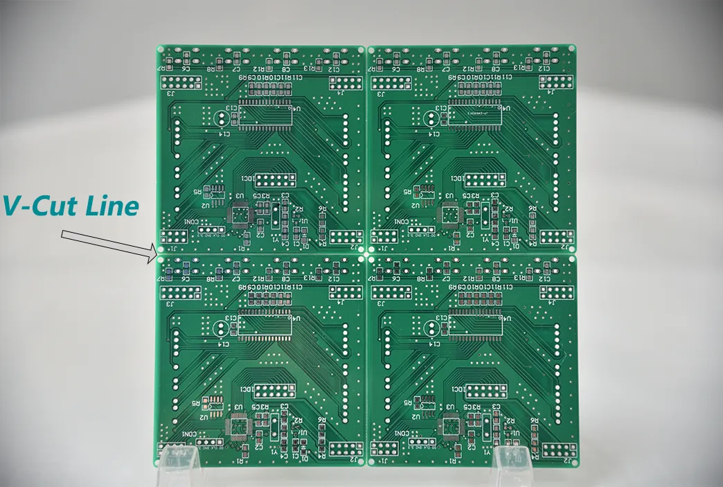
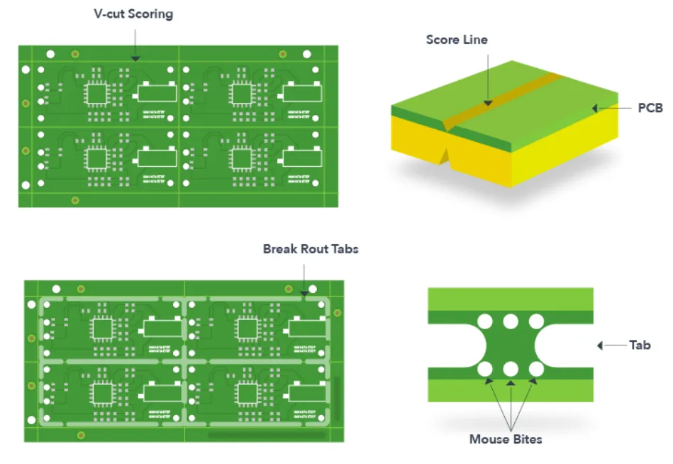
V-scoring, also known as V-cut, is a method used to create a groove along the edges of individual PCBs within a panel. This groove weakens the material just enough to allow easy separation by hand or with minimal force after assembly. The "V" shape of the cut—typically at a 30 to 45-degree angle—ensures precision and reduces stress on the board during separation.
For engineers focusing on V-scoring panel layout, this technique is ideal for rectangular or square boards. It’s cost-effective compared to other methods like routing (which involves cutting out tabs with a CNC machine) and works well for high-volume production. However, V-scoring isn’t suitable for complex shapes or designs with components close to the edge, as the scoring process can cause stress or damage.
Benefits of V-Scoring for PCB Manufacturability
When it comes to V-scoring manufacturability, this method offers several advantages that align with efficient production goals. Let’s break down the key benefits:
- Cost Efficiency: V-scoring requires less equipment setup and processing time compared to routing. This translates to lower manufacturing costs, especially for large batches.
- Speed: Scoring machines can create grooves quickly across an entire panel, speeding up the production process.
- Clean Separation: When done correctly, V-scoring results in clean edges with minimal burring or residue, reducing the need for post-processing.
- Compatibility with Automation: V-scored panels are easy to handle in automated assembly lines, as they maintain structural integrity until separation is needed.
By incorporating V-scoring into your design, you can achieve a balance between production efficiency and board quality. However, careful planning is essential to avoid issues like misalignment or excessive stress during separation.
Best Practices for V-Scoring Design for Manufacturing (DFM)
Designing with V-scoring design for manufacturing (DFM) principles in mind ensures that your PCB panelization process is optimized from the start. Here are some best practices to follow:
1. Maintain Proper Spacing Between Boards
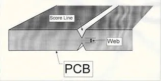
For V-scoring to work effectively, there must be enough space between individual PCBs on the panel. A common guideline is to leave at least 0.3 mm to 0.5 mm of material between boards after scoring. This residual material, often called the "web," holds the panel together during manufacturing but allows for easy separation later. Too thin a web can lead to accidental breakage during handling, while too thick a web makes separation difficult.
2. Avoid Components Near Score Lines
Placing components too close to the V-score line can result in damage during scoring or separation. As a rule of thumb, keep components at least 5 mm away from the score line. This buffer zone protects sensitive parts from mechanical stress and ensures the integrity of solder joints.
3. Use Standard Board Thicknesses
V-scoring works best with standard PCB thicknesses, typically between 0.6 mm and 2.0 mm. Thicker boards (above 2.4 mm) may require deeper grooves, which can weaken the panel excessively. Thinner boards (below 0.6 mm) might not withstand the scoring process without cracking. Always confirm the capabilities of your manufacturing partner regarding board thickness and scoring depth.
4. Align Score Lines with Board Edges
For rectangular boards, ensure that V-score lines run parallel to the edges and span the entire length or width of the panel. Misaligned or partial scoring can lead to uneven separation, resulting in jagged edges or damaged boards. Most manufacturers recommend that score lines extend at least 5 mm beyond the panel’s process edges to guarantee a clean cut.
5. Consider Panel Strength During Assembly
While V-scoring weakens the panel for separation, it must still maintain enough strength to withstand handling and assembly processes. A common practice is to leave a web thickness of about 1/3 of the board’s total thickness. For a 1.6 mm thick board, this means a web of approximately 0.5 mm. This balance ensures stability without making de-panelization too difficult.
Common Challenges in V-Scoring and How to Avoid Them
While V-scoring is a reliable method for PCB panelization, it’s not without challenges. Being aware of potential issues can help you design better layouts and avoid costly mistakes. Here are some common problems and solutions:
1. Board Warpage or Stress
Improper scoring depth or web thickness can cause the panel to warp or induce stress, especially in thinner boards. To prevent this, ensure the scoring depth is consistent—typically 1/3 of the board thickness on each side (top and bottom). For a 1.6 mm board, this means a scoring depth of about 0.5 mm per side, leaving a 0.6 mm web in the center.
2. Misaligned Score Lines
If the top and bottom score lines are not perfectly aligned, separation becomes uneven, leading to rough edges or board damage. Work closely with your manufacturer to confirm their scoring precision, often within a tolerance of ±0.1 mm, to ensure alignment.
3. Damage to Edge Components
As mentioned earlier, components too close to the score line are at risk. Beyond maintaining a 5 mm clearance, consider adding fiducial marks or tooling holes to guide scoring accuracy and protect critical areas.
4. Incompatibility with Complex Designs
V-scoring is not ideal for boards with irregular shapes or cutouts near the edges. In such cases, consider alternative methods like tab routing, where small breakaway tabs hold the board in place and are later removed. While routing is more expensive, it offers greater flexibility for non-standard designs.
Integrating V-Scoring into Your PCB Panelization Workflow
To fully leverage V-scoring in your PCB panelization process, it’s essential to integrate it into your design workflow from the beginning. Start by collaborating with your manufacturing partner to understand their specific V-scoring capabilities and limitations. Many manufacturers provide design guidelines that specify minimum web thickness, scoring angles (often 30° or 45°), and tolerances.
Next, use PCB design software to mark V-score lines clearly in your layout files. Most tools allow you to add these lines as a separate layer, ensuring they’re visible to the manufacturer. Label them explicitly as “V-score” or “V-cut” in your documentation to avoid confusion with other cut lines or features.
Finally, perform a design review focused on V-scoring design for manufacturing (DFM). Check for component placement, board spacing, and score line alignment. Running a DFM analysis can catch potential issues before production, saving time and reducing the risk of costly re-spins.
Comparing V-Scoring to Other Panelization Methods
While V-scoring is a popular choice for many projects, it’s worth comparing it to other de-panelization methods to determine the best fit for your design. Here’s a quick overview:
- V-Scoring: Best for rectangular boards, cost-effective, and fast. Limited to straight lines and may stress components near edges.
- Tab Routing: Ideal for irregular shapes, offers precise control over separation points. More expensive due to CNC machining and slower processing.
- Mouse Bites: Uses a series of small holes to create weak points for separation. Suitable for small boards or prototypes but leaves rough edges and requires manual cleanup.
For most standard designs, V-scoring strikes a balance between cost and ease of use, making it a go-to option for engineers focused on V-scoring manufacturability.
Final Tips for Optimizing PCB Panelization with V-Scoring
As you refine your approach to PCB panelization and V-scoring, keep these final tips in mind to maximize efficiency and quality:
- Always request a panelization drawing from your manufacturer before production to confirm V-score placement and panel layout.
- Test a small batch of panels to validate separation ease and board integrity, especially for new designs.
- Document all V-scoring specifications in your design files, including web thickness, scoring depth, and angle, to ensure consistency across production runs.
- Stay updated on industry standards for panelization and DFM to incorporate the latest best practices into your workflow.
Conclusion: Mastering V-Scoring for Better PCB Production
Optimizing PCB panelization with V-scoring is a powerful way to enhance manufacturing efficiency, reduce costs, and ensure high-quality results. By focusing on V-scoring panel layout, prioritizing V-scoring manufacturability, and adhering to V-scoring design for manufacturing (DFM) guidelines, engineers can streamline the transition from design to production. With the right planning and collaboration with your manufacturing partner, V-scoring can become a cornerstone of your PCB production strategy, delivering reliable and cost-effective outcomes for projects of any scale.
Armed with the insights and best practices from this guide, you’re ready to tackle your next PCB project with confidence. Focus on precision in your designs, and let V-scoring help you achieve seamless panelization and de-panelization every time.


