 ALLPCB


Are you new to PCB fabrication and curious about laser drilling? Laser drilling is a cutting-edge technique used to create precise holes and vias in printed circuit boards (PCBs), offering unmatched accuracy for modern electronics. In this guide, we'll cover laser drilling PCB basics, the PCB fabrication process, laser drilling advantages for hobbyists, tips for choosing a laser for PCB drilling, and how to set up a PCB laser drilling setup for home use. Whether you're a hobbyist or an aspiring engineer, this introductory guide will help you understand the essentials and get started with confidence.
Let’s dive into the world of laser drilling and explore how it transforms PCB fabrication with precision and efficiency.
What Is Laser Drilling in PCB Fabrication?
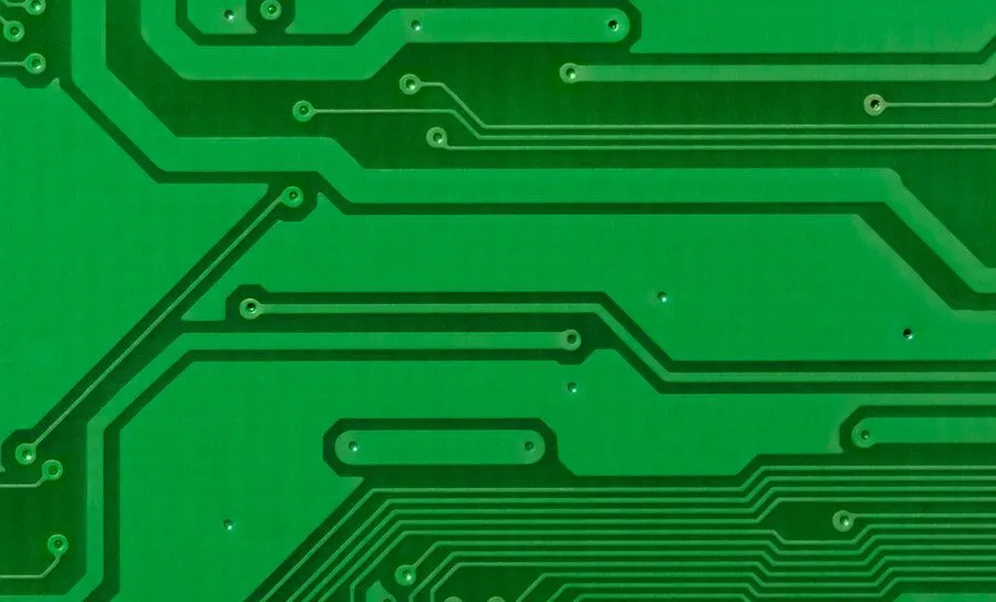
Laser drilling is a non-contact process that uses a focused laser beam to create holes, known as vias, in a PCB. Unlike traditional mechanical drilling, which uses physical bits, laser drilling vaporizes material with intense heat, allowing for smaller, more precise holes. This method is especially critical for high-density interconnect (HDI) boards, where space is limited, and accuracy is paramount.
In the context of PCB fabrication, laser drilling is often used to create microvias—tiny holes typically less than 0.15 mm (6 mils) in diameter—that connect different layers of a multilayer PCB. These microvias enable the compact designs found in smartphones, wearables, and other advanced electronics.
Understanding the PCB Fabrication Process: A Step-by-Step Overview
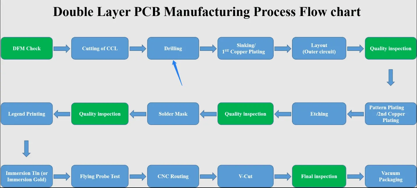
Before diving deeper into laser drilling, it’s important to understand the broader PCB fabrication process. This process transforms a design into a functional circuit board through several key stages. Here’s a simplified breakdown for beginners:
- Design and Layout: The process starts with creating a digital blueprint of the PCB using design software. This includes defining the placement of components, traces, and vias.
- Material Preparation: A substrate, often made of fiberglass (FR-4), is prepared and coated with a thin layer of copper on one or both sides.
- Etching: Unwanted copper is removed using chemicals to form the circuit pattern based on the design.
- Drilling: Holes for vias and component leads are created. This is where laser drilling comes into play for precision microvias, while mechanical drilling may be used for larger holes.
- Plating: The drilled holes are plated with copper to establish electrical connections between layers in multilayer boards.
- Solder Mask and Silkscreen: A protective solder mask is applied to prevent short circuits, and a silkscreen layer adds labels and markings.
- Testing: The finished PCB undergoes electrical testing to ensure functionality before assembly.
Laser drilling fits into the drilling stage, offering a modern alternative to mechanical methods for creating smaller, more precise holes. Its role is critical in achieving the high-density designs required for today’s electronics.
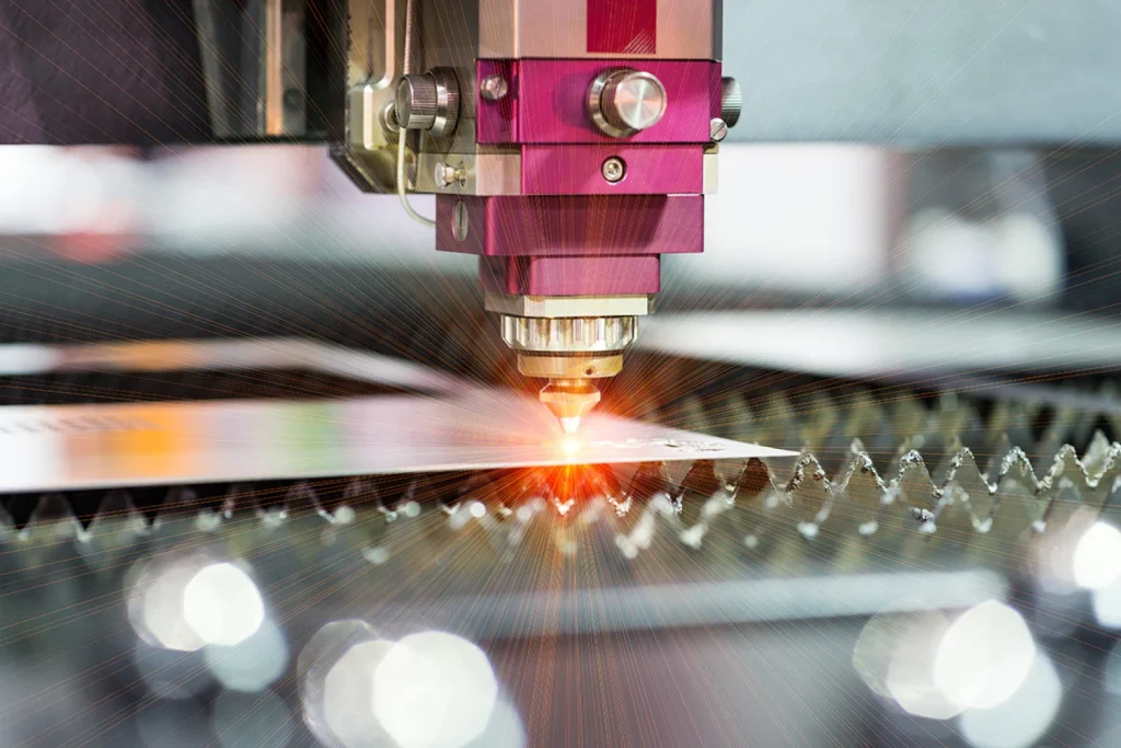
Laser Drilling PCB Basics: How It Works
Let’s break down the laser drilling PCB basics to help beginners grasp the concept. Laser drilling uses a concentrated beam of light to remove material from the PCB substrate. Here’s how the process typically works:
- Laser Beam Focus: A laser, often a CO2 or UV type, emits a beam that is focused onto the PCB surface using lenses. The beam’s diameter can be as small as 0.025 mm (1 mil) for ultra-fine holes.
- Material Removal: The intense heat from the laser vaporizes or ablates the material, creating a clean hole without physical contact. This minimizes the risk of damage to the board.
- Control and Precision: Advanced systems control the laser’s power, pulse duration, and position to achieve specific hole sizes and depths. For instance, microvias in HDI boards often have depths of 0.05 to 0.1 mm.
- Debris Management: During drilling, debris is removed using air or vacuum systems to prevent contamination of the PCB surface.
This process is ideal for creating blind vias (holes that don’t go through the entire board) and buried vias (holes within internal layers), which are essential for multilayer PCB designs.
Laser Drilling Advantages for Hobbyists
For hobbyists venturing into PCB design and fabrication, laser drilling offers several compelling benefits. Here’s why laser drilling advantages for hobbyists make it an attractive option:
- Precision for Small Projects: Hobbyists often work on compact designs where space is limited. Laser drilling can create microvias with diameters as small as 0.1 mm, allowing for denser layouts without sacrificing quality.
- No Mechanical Stress: Unlike mechanical drilling, which can cause cracks or delamination in thin or fragile boards, laser drilling is a non-contact process that reduces the risk of physical damage.
- Versatility: Laser systems can handle a variety of materials, including standard FR-4, flexible substrates, and even ceramics, giving hobbyists flexibility in their projects.
- Reduced Tool Wear: Mechanical drill bits wear out over time and need frequent replacement, adding to costs. A laser system, while initially more expensive, doesn’t require consumable tools for drilling.
- Improved Learning Opportunities: Using advanced technology like laser drilling helps hobbyists gain hands-on experience with modern fabrication techniques, preparing them for more complex projects or professional roles.
While the upfront cost of laser equipment may seem high, the long-term benefits of precision and versatility can outweigh the investment for serious hobbyists.
Choosing a Laser for PCB Drilling: Key Factors to Consider
When it comes to choosing a laser for PCB drilling, beginners and hobbyists need to evaluate several factors to ensure they select the right equipment for their needs. Here are the main considerations:
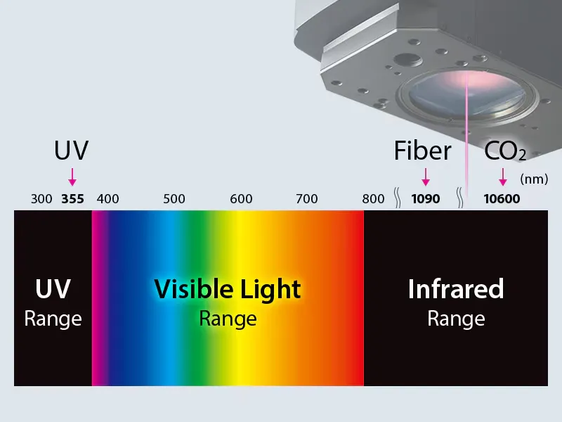
- Type of Laser: CO2 lasers are commonly used for drilling through organic materials like FR-4, with wavelengths around 10.6 micrometers. UV lasers, with wavelengths of 355 nm, are better for finer precision and drilling through copper or mixed materials. Choose based on your PCB material and hole size requirements.
- Power Output: Laser power, measured in watts, affects drilling speed and capability. For hobbyist use, a 10-20 watt laser may suffice for thin boards, while thicker or multilayer boards may require 30 watts or more.
- Control Software: Look for systems with user-friendly software that allows you to adjust parameters like beam focus, pulse duration, and drilling depth. Compatibility with PCB design files (e.g., Gerber format) is also essential.
- Safety Features: Lasers pose risks like eye damage and fire hazards. Ensure the system includes safety enclosures, emergency stop buttons, and proper ventilation to handle fumes.
- Cost and Scalability: Entry-level laser systems for hobbyists can range from $1,000 to $5,000, while industrial-grade machines cost much more. Start with a budget-friendly option that can be upgraded as your skills grow.
By carefully assessing these factors, you can select a laser system that matches your project goals and skill level.
PCB Laser Drilling Setup for Home Use: A Beginner’s Guide
Setting up a PCB laser drilling setup for home use may seem daunting, but with the right tools and precautions, it’s achievable for hobbyists. Follow these steps to create a safe and effective workspace:
- Choose a Suitable Space: Set up your laser in a well-ventilated area, away from flammable materials. A garage or dedicated workshop with a sturdy workbench is ideal.
- Acquire Essential Equipment: You’ll need a laser system (based on the criteria above), a computer with control software, and a fixture to hold the PCB steady during drilling. A simple vise or custom jig can work for small boards.
- Install Safety Measures: Use laser safety goggles rated for the specific wavelength of your laser. Enclose the drilling area with a protective shield to contain stray beams, and install a smoke extractor to remove fumes generated during drilling.
- Prepare Your PCB: Secure the PCB in the fixture, ensuring it’s level. Upload your design file to the laser control software, and double-check the alignment of drilling locations.
- Test and Calibrate: Start with a test piece of scrap material to calibrate the laser’s focus and power settings. For example, set the power to 15 watts and adjust pulse duration to 10 microseconds for a 0.1 mm hole in FR-4 material.
- Drill and Inspect: Run the laser drilling process, monitoring for any issues. After completion, inspect the holes under a magnifying glass to ensure they meet the desired diameter and depth.
Always follow manufacturer guidelines for your specific laser system, and never bypass safety protocols. With practice, you’ll gain confidence in creating precise vias for your PCB projects at home.
Challenges and Tips for Laser Drilling in PCB Fabrication
While laser drilling offers many benefits, it’s not without challenges, especially for beginners. Here are some common issues and tips to overcome them:
- Heat Damage: Excessive heat from the laser can cause charring or delamination of the PCB material. Use lower power settings and shorter pulse durations to minimize heat buildup.
- Alignment Issues: Misaligned holes can ruin a PCB design. Always double-check the positioning in your software and use a high-quality fixture to hold the board steady.
- Cost of Equipment: Laser systems can be expensive for hobbyists. Consider starting with a shared makerspace or community workshop that offers access to laser tools before investing in your own.
- Learning Curve: Operating a laser system takes time to master. Watch online tutorials, read user manuals, and start with simple projects to build your skills.
By anticipating these challenges and applying these tips, you can achieve better results with laser drilling over time.
Conclusion: Why Laser Drilling Is the Future for PCB Hobbyists
Laser drilling is revolutionizing PCB fabrication with its precision, versatility, and ability to meet the demands of modern electronics. For beginners and hobbyists, understanding laser drilling PCB basics and the PCB fabrication process opens up new possibilities for creating compact, high-performance circuit boards. The laser drilling advantages for hobbyists—such as accuracy and reduced mechanical stress—make it a worthwhile skill to learn, while choosing a laser for PCB drilling and setting up a PCB laser drilling setup for home use can be done with careful planning and the right equipment.
At ALLPCB, we’re committed to supporting your journey in PCB design and fabrication. Whether you’re experimenting at home or scaling up to professional projects, laser drilling offers a powerful tool to bring your ideas to life. Start small, prioritize safety, and embrace the learning process to master this innovative technology.


